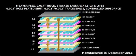
What are HDI PCB Stackups?
HDI PCB stackups refer to the arrangement of copper layers and dielectric materials in an HDI PCB. The numbers in the stackup notation represent the number of copper layers on each side of the core material (N). For example, a 1+N+1 stackup has one copper layer on each side of the core, while a 4+N+4 stackup has four copper layers on each side.
The most common HDI PCB stackups are:
- 1+N+1
- 2+N+2
- 3+N+3
- 4+N+4
Advantages of HDI PCB Stackups
HDI PCB stackups offer several benefits compared to conventional PCBs:
- Higher component density
- Improved signal integrity
- Reduced form factor
- Enhanced thermal management
- Lower power consumption
One-Stop HDI PCB Manufacturing Process
The one-stop HDI PCB manufacturing process involves several stages, from design to final assembly. By consolidating all these stages under one roof, manufacturers can ensure better quality control, faster turnaround times, and cost-effectiveness.
1. Design and Prototyping
The first step in HDI PCB manufacturing is the design and prototyping phase. This involves creating the schematic diagram, PCB layout, and generating Gerber files. The design team works closely with the customer to ensure that the PCB meets all the required specifications and standards.
2. Material Selection
Selecting the right materials is crucial for the performance and reliability of HDI PCBs. The common materials used in HDI PCB manufacturing are:
- FR-4: A glass-reinforced epoxy laminate material
- Polyimide: A high-temperature resistant polymer
- Rogers: A high-frequency laminate material
The choice of material depends on the specific application and the required electrical, thermal, and mechanical properties.
3. Fabrication
The fabrication stage involves several sub-processes, such as:
a. Drilling: Creating holes in the PCB for component placement and via formation.
b. Plating: Depositing a thin layer of copper on the drilled holes to create electrical connections between layers.
c. Patterning: Transferring the PCB layout onto the copper layers using photolithography.
d. Etching: Removing unwanted copper to create the desired circuit pattern.
e. Lamination: Bonding the copper layers and dielectric materials together under high temperature and pressure.
4. Solder Mask Application
A solder mask is a protective coating applied to the PCB surface to prevent solder bridging and protect the copper traces from oxidation. The solder mask is typically green in color but can be customized according to the customer’s requirements.
5. Surface Finish
The surface finish is a thin layer of metal applied to the exposed copper pads to prevent oxidation and improve solderability. The common surface finishes used in HDI PCB manufacturing are:
- HASL (Hot Air Solder Leveling)
- ENIG (Electroless Nickel Immersion Gold)
- OSP (Organic Solderability Preservative)
- Immersion Silver
- Immersion Tin
The choice of surface finish depends on the specific application, the Component Types, and the soldering process.
6. Electrical Testing
After the fabrication and finishing processes, the HDI PCBs undergo rigorous electrical testing to ensure that they meet the required specifications and standards. This includes continuity testing, insulation resistance testing, and high-potential testing.
7. Assembly
The final stage in the one-stop HDI PCB manufacturing process is assembly. This involves soldering the components onto the PCB using either through-hole or Surface-mount technology (SMT). The assembled PCBs are then subjected to further testing and inspection to ensure that they function as intended.

HDI PCB Stackup Comparison
The choice of HDI PCB stackup depends on the specific application, the required performance, and the cost constraints. The following table compares the different HDI PCB stackups based on various parameters:
| Stackup | Layers | Density | Signal Integrity | Cost |
|---|---|---|---|---|
| 1+N+1 | 2-4 | Low | Good | Low |
| 2+N+2 | 4-8 | Medium | Better | Medium |
| 3+N+3 | 6-12 | High | Best | High |
| 4+N+4 | 8-16 | Very High | Excellent | Very High |
As evident from the table, higher stackups offer better density and signal integrity but come at a higher cost. The choice of stackup ultimately depends on finding the right balance between performance and cost for the specific application.

Frequently Asked Questions (FAQ)
-
What is the difference between HDI PCBs and conventional PCBs?
HDI PCBs have higher component density, improved signal integrity, and smaller form factors compared to conventional PCBs. They achieve this by using smaller vias, finer trace widths, and thinner dielectric materials. -
What are microvias, and how are they used in HDI PCBs?
Microvias are small vias with a diameter less than 150 µm. They are used in HDI PCBs to create high-density interconnects between layers. Microvias can be formed using laser drilling, photovia, or conductive paste filling techniques. -
What are the challenges in manufacturing HDI PCBs?
Manufacturing HDI PCBs requires advanced equipment, skilled personnel, and stringent process control. Some of the challenges include maintaining tight tolerances, ensuring reliable via formation, and managing signal integrity issues. -
How do I choose the right HDI PCB stackup for my application?
The choice of HDI PCB stackup depends on several factors, such as the required component density, signal integrity, thermal management, and cost constraints. It is advisable to consult with an experienced HDI PCB manufacturer to determine the optimal stackup for your specific application. -
What are the benefits of using a one-stop HDI PCB manufacturing service?
A one-stop HDI PCB manufacturing service offers several benefits, such as better quality control, faster turnaround times, and cost-effectiveness. By consolidating all the manufacturing stages under one roof, the manufacturer can ensure seamless communication, minimize errors, and optimize the production process.

Conclusion
HDI PCBs have become indispensable in modern electronics manufacturing due to their ability to deliver high performance in a compact form factor. The one-stop HDI PCB manufacturing process enables customers to get their HDI PCBs manufactured efficiently and cost-effectively. By understanding the different HDI PCB stackups and their advantages, designers can make informed decisions and choose the right stackup for their specific applications. As technology continues to advance, the demand for HDI PCBs is expected to grow, driving further innovations in materials, processes, and equipment.


Leave a Reply