What is a PCB Stackup?
A printed circuit board (PCB) stackup refers to the arrangement of copper and insulating layers that make up a PCB. The stackup defines the number of layers, the thickness of each layer, the materials used, and the interconnections between layers. The stackup is a critical design element that impacts many aspects of PCB Performance, manufacturability, and reliability.
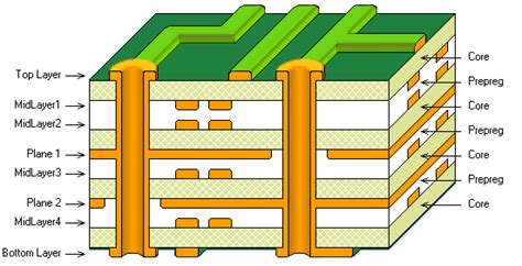
In a typical Multilayer PCB stackup, the layers alternate between conductor (copper) and insulator (dielectric). The outer layers are usually conductor layers, while inner layers can be conductor or insulator depending on the design. Multilayer PCBs provide several advantages over simpler double-layer boards, including:
- Increased routing density and design flexibility
- Better signal integrity and EMI performance
- Improved power delivery and heat dissipation
- Smaller form factors and higher reliability
However, multilayer stackups also introduce new challenges and tradeoffs that must be carefully considered during the design process. Factors such as the layer count, material selection, trace widths and spacings, via spans, and impedance requirements can significantly affect the manufacturability, cost, and performance of the final board.
Standard Multilayer PCB Stackups
While the exact number and arrangement of layers in a multilayer PCB can vary widely depending on the specific application and design constraints, there are some common stackup configurations that are widely used in the industry. These standard stackups offer a good balance of performance, manufacturability, and cost for a wide range of applications.
4-Layer Stackup
The 4-layer stackup is one of the most common configurations for moderate-complexity designs. It offers a good balance of routing density, signal integrity, and power delivery in a relatively low-cost and easy-to-manufacture package.
A typical 4-layer stackup consists of the following layers:
| Layer | Material | Thickness (mils) |
|---|---|---|
| Top | Copper | 1.4 |
| Core | FR-4 | 8.0 |
| Inner 1 | Copper | 1.0 |
| Inner 2 | Copper | 1.0 |
| Core | FR-4 | 47.0 |
| Bottom | Copper | 1.4 |
The top and bottom layers are used for component placement and routing, while the inner layers are typically used for power and ground planes. The core layers provide mechanical stability and insulation between the conductor layers.
6-Layer Stackup
For more complex designs that require higher routing density or better signal integrity, a 6-layer stackup may be used. This configuration adds two additional inner conductor layers, providing more flexibility for signal routing and power delivery.
A typical 6-layer stackup looks like this:
| Layer | Material | Thickness (mils) |
|---|---|---|
| Top | Copper | 1.4 |
| Prepreg | FR-4 | 4.0 |
| Inner 1 | Copper | 1.0 |
| Core | FR-4 | 40.0 |
| Inner 2 | Copper | 1.0 |
| Prepreg | FR-4 | 4.0 |
| Inner 3 | Copper | 1.0 |
| Core | FR-4 | 40.0 |
| Inner 4 | Copper | 1.0 |
| Prepreg | FR-4 | 4.0 |
| Bottom | Copper | 1.4 |
In this stackup, the inner layers are typically arranged as signal-ground-signal-ground to provide good signal integrity and EMI performance. The prepreg layers are thin sheets of pre-impregnated fiberglass used to bond the inner layers together.
8-Layer and Beyond
For very high-density or high-speed designs, 8-layer or even 10+ layer stackups may be necessary. These configurations provide maximum routing density and signal integrity, but at the cost of increased manufacturing complexity and expense.
A typical 8-layer stackup might look like this:
| Layer | Material | Thickness (mils) |
|---|---|---|
| Top | Copper | 1.4 |
| Prepreg | FR-4 | 3.6 |
| Inner 1 | Copper | 0.7 |
| Prepreg | FR-4 | 6.7 |
| Inner 2 | Copper | 0.7 |
| Core | FR-4 | 37.4 |
| Inner 3 | Copper | 0.7 |
| Prepreg | FR-4 | 6.7 |
| Inner 4 | Copper | 0.7 |
| Prepreg | FR-4 | 3.6 |
| Inner 5 | Copper | 0.7 |
| Core | FR-4 | 37.4 |
| Inner 6 | Copper | 0.7 |
| Prepreg | FR-4 | 3.6 |
| Bottom | Copper | 1.4 |
In this configuration, the inner layers are arranged in a stripline structure to maximize signal integrity and minimize crosstalk. The multiple ground planes also provide excellent power delivery and shielding.
For even higher layer counts, the stackup design becomes increasingly application-specific, and may require advanced materials, microvias, or other specialized technologies to achieve the desired performance and reliability.

PCB Material Selection
In addition to the number and arrangement of layers, the choice of materials used in the PCB stackup can have a significant impact on the board’s performance and manufacturability. The most common materials used in PCB fabrication are:
FR-4
FR-4 (Flame Retardant 4) is a glass-reinforced epoxy laminate material that is widely used as the base material for PCBs. It offers a good balance of mechanical, electrical, and thermal properties at a relatively low cost. FR-4 is available in a variety of grades and thicknesses to suit different applications.
High-Frequency Laminates
For high-speed or high-frequency applications, specialized laminate materials may be used to provide better dielectric properties and lower losses. Examples include Rogers, Isola, and Nelco materials, which offer lower dielectric constants and loss tangents than standard FR-4.
Copper Foils
The copper foils used in PCBs come in different weights (thicknesses) and types (electrodeposited or rolled-annealed). The choice of copper foil can affect the achievable trace geometries, current carrying capacity, and signal integrity of the board.
Solder Mask
Solder mask is a polymer coating applied over the outer layers of the PCB to protect the copper traces from oxidation and prevent solder bridging. It is available in different colors (green, red, blue, etc.) and finishes (matte or glossy).
Surface Finish
The surface finish is a thin layer of metal applied over the exposed copper pads to prevent oxidation and improve solderability. Common surface finishes include HASL (hot air solder leveling), ENIG (electroless nickel immersion gold), and OSP (organic solderability preservative).

Stackup Design Considerations
When designing a PCB stackup, there are several key factors to consider in order to achieve the desired performance, manufacturability, and cost targets:
Layer Count
The number of layers in the stackup should be chosen based on the routing density, signal integrity, and power delivery requirements of the design. Higher layer counts provide more routing flexibility and better performance, but at the cost of increased manufacturing complexity and expense.
Material Selection
The choice of materials used in the stackup should be based on the electrical, mechanical, and thermal requirements of the application. Factors to consider include the dielectric constant, loss tangent, glass transition temperature, and coefficient of thermal expansion of the laminate materials.
Trace Geometry
The width and spacing of the copper traces on each layer should be designed to achieve the desired impedance, current carrying capacity, and manufacturability. Thinner traces allow for higher routing density, but may be more difficult to manufacture reliably.
Via Spans
The number and arrangement of vias (plated through-holes) used to interconnect the layers should be carefully considered to minimize the impact on routing density and signal integrity. Blind and buried vias can be used to improve layer-to-layer connectivity, but may increase manufacturing cost and complexity.
Impedance Control
For high-speed or impedance-controlled designs, the stackup should be designed to achieve the desired characteristic impedance of the traces. This requires careful selection of the dielectric materials and thicknesses, as well as precise control of the trace geometries.
EMI/EMC
The stackup design can have a significant impact on the electromagnetic interference (EMI) and compatibility (EMC) performance of the PCB. Proper layer arrangement, grounding, and shielding techniques can help minimize EMI and ensure compliance with regulatory standards.

PCB Stackup Documentation
Once the stackup design is finalized, it is important to document it clearly and communicate it to the PCB fabricator. The stackup documentation should include:
- A cross-sectional diagram showing the arrangement of layers, materials, and thicknesses
- A table specifying the material type, thickness, and copper weight for each layer
- Notes on any special requirements, such as impedance control or surface finish
- Dimensional tolerances and acceptable variances for each parameter
Clear and accurate stackup documentation helps ensure that the PCB fabricator can manufacture the board to the desired specifications and avoid costly errors or delays.
FAQ
What is the most common PCB stackup?
The most common PCB stackup is the 4-layer configuration, which consists of top and bottom signal layers, and two inner power/ground layers. This stackup provides a good balance of routing density, signal integrity, and power delivery for many applications.
How many layers can a PCB have?
In theory, a PCB can have any number of layers, but in practice, most designs use between 2 and 16 layers. Higher layer counts are possible, but may require specialized materials and manufacturing processes that increase cost and complexity.
What is the difference between a core and prepreg layer?
A core layer is a thick, pre-cured laminate material that provides mechanical stability and insulation between the conductor layers. A prepreg (pre-impregnated) layer is a thin sheet of uncured fiberglass and resin that is used to bond the core and conductor layers together during the lamination process.
How does the PCB stackup affect signal integrity?
The PCB stackup can have a significant impact on signal integrity, particularly for high-speed or high-frequency designs. The dielectric constant and loss tangent of the laminate materials, the thickness and spacing of the copper layers, and the arrangement of power and ground planes all affect the propagation speed, impedance, and crosstalk of signals on the board.
What is the typical turnaround time for a multilayer PCB?
The turnaround time for a multilayer PCB depends on the complexity of the design, the materials and processes used, and the workload of the fabricator. For a standard 4-6 layer board, the typical lead time is 1-2 weeks, but this can vary widely depending on the specific requirements and circumstances of the project. Rush services and expedited options may be available for an additional cost.


Leave a Reply