Introduction to Multilayer PCBs
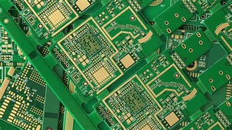
A Multilayer PCB, or Multilayer Printed Circuit Board, is a complex circuit board that consists of multiple layers of conductive copper foil laminated together with insulating material. These layers are interconnected through carefully drilled holes called vias, allowing for intricate electrical connections between different layers. Multilayer PCBs have become increasingly popular in modern electronics due to their ability to accommodate high component density, improve signal integrity, and reduce electromagnetic interference (EMI).
Definition of Multilayer PCB
A Multilayer PCB is defined as a printed circuit board that contains three or more conductive copper layers, separated by insulating layers, and interconnected through vias. The number of layers in a Multilayer PCB can vary depending on the complexity of the circuit design, with some boards having up to 50 layers or more.
Advantages of Multilayer PCBs
Multilayer PCBs offer several advantages over traditional single or double-layer PCBs:
- Increased component density: With multiple layers, designers can accommodate more components and complex circuitry in a smaller footprint.
- Improved signal integrity: By carefully routing signals through different layers and utilizing proper grounding techniques, Multilayer PCBs can minimize signal interference and maintain signal integrity.
- Reduced EMI: The use of ground planes and proper layer arrangement can help reduce electromagnetic interference, making Multilayer PCBs suitable for sensitive electronic applications.
- Enhanced thermal management: Multilayer PCBs can incorporate dedicated layers for heat dissipation, improving the overall thermal performance of the board.
Multilayer PCB Manufacturing Process
The manufacturing process for Multilayer PCBs is more complex than that of single or double-layer boards. It involves several key steps:
1. Layer Preparation
The process begins with the preparation of individual layers. Each layer consists of a thin copper foil laminated onto an insulating substrate material, typically FR-4. The copper foil is coated with a photoresist material, which is then exposed to UV light through a photomask containing the desired circuit pattern. The unexposed photoresist is then removed, leaving behind the desired copper traces.
2. Layer Stacking and Lamination
Once the individual layers are prepared, they are stacked together in the proper sequence, with insulating material placed between each layer. The stack is then subjected to high pressure and temperature in a lamination press, bonding the layers together to form a solid board.
3. Drilling and Plating
After lamination, holes are drilled through the board at specific locations to create vias. These holes are then plated with copper to establish electrical connections between layers. Additional drilling may be performed to create mounting holes or other features.
4. Outer Layer Processing
The outer layers of the Multilayer PCB undergo additional processing, which includes applying a solder mask to protect the copper traces and adding silkscreen legends for component placement and identification. Surface finishes, such as HASL (Hot Air Solder Leveling) or ENIG (Electroless Nickel Immersion Gold), are applied to the exposed copper areas to improve solderability and protect against oxidation.
5. Inspection and Testing
Throughout the manufacturing process, various inspections and tests are performed to ensure the quality and functionality of the Multilayer PCB. These may include visual inspections, electrical continuity tests, and impedance measurements.

Multilayer PCB Design Considerations
Designing a Multilayer PCB requires careful consideration of several factors to ensure optimal performance and manufacturability:
1. Layer Stack-up
The arrangement of layers in a Multilayer PCB, known as the layer stack-up, is crucial for signal integrity and EMI control. A typical stack-up includes signal layers, power planes, and ground planes. Signal layers are used for routing traces, while power and ground planes provide stable reference voltages and help reduce EMI.
2. Via Types and Placement
Vias are essential for interconnecting different layers in a Multilayer PCB. There are several types of vias, including through-hole vias, blind vias, and buried vias. Through-hole vias extend through the entire thickness of the board, while blind and buried vias connect only certain layers. Via placement and size must be carefully considered to minimize signal integrity issues and ensure manufacturability.
3. Trace Width and Spacing
The width and spacing of traces on a Multilayer PCB must be carefully designed to maintain signal integrity and avoid crosstalk. Factors such as the operating frequency, impedance requirements, and manufacturing capabilities must be taken into account when determining trace dimensions.
4. Grounding and Shielding
Proper grounding and shielding techniques are essential for controlling EMI and maintaining signal integrity in Multilayer PCBs. This includes the use of ground planes, stitching vias, and shielding cans or enclosures.
5. Thermal Management
As Multilayer PCBs often accommodate high component density, thermal management becomes a critical design consideration. Designers must ensure adequate heat dissipation through the use of thermal vias, copper pours, and appropriate layer placement.

Applications of Multilayer PCBs
Multilayer PCBs find applications in a wide range of industries and products, including:
- Consumer Electronics: Smartphones, tablets, laptops, and wearable devices.
- Automotive Electronics: Engine control units, infotainment systems, and advanced driver assistance systems (ADAS).
- Medical Devices: Implantable devices, diagnostic equipment, and patient monitoring systems.
- Aerospace and Defense: Avionics, satellite communication systems, and military equipment.
- Industrial Automation: Programmable logic controllers (PLCs), human-machine interfaces (HMIs), and industrial control systems.

Frequently Asked Questions (FAQ)
1. What is the difference between a Multilayer PCB and a single or double-layer PCB?
A Multilayer PCB consists of three or more conductive layers, while single and double-layer PCBs have one or two conductive layers, respectively. Multilayer PCBs offer increased component density, improved signal integrity, and better EMI control compared to single or double-layer boards.
2. How many layers can a Multilayer PCB have?
The number of layers in a Multilayer PCB can vary depending on the complexity of the circuit design and the specific application requirements. Some Multilayer PCBs may have as few as four layers, while others can have up to 50 layers or more.
3. What materials are used in the construction of Multilayer PCBs?
Multilayer PCBs typically use a combination of copper foil for the conductive layers and FR-4 (Flame Retardant 4) as the insulating substrate material. Other materials, such as polyimide or high-frequency laminates, may be used for specific applications or performance requirements.
4. What are vias, and why are they important in Multilayer PCBs?
Vias are holes drilled through a Multilayer PCB that are plated with copper to create electrical connections between different layers. They are essential for routing signals and power between layers, allowing for complex circuitry in a compact form factor.
5. How can I ensure the manufacturability of my Multilayer PCB design?
To ensure the manufacturability of a Multilayer PCB design, consider factors such as layer stack-up, via types and placement, trace width and spacing, and thermal management. Consult with your PCB manufacturer early in the design process to discuss design rules, constraints, and best practices specific to their manufacturing capabilities.
Conclusion
Multilayer PCBs have revolutionized the electronics industry by enabling the development of compact, high-performance devices with complex functionality. By leveraging the advantages of multiple conductive layers, designers can create circuits with increased component density, improved signal integrity, and reduced EMI. However, the design and manufacture of Multilayer PCBs require careful consideration of various factors, such as layer stack-up, via placement, trace dimensions, grounding, and thermal management.
As technology continues to advance, the demand for Multilayer PCBs is expected to grow across various industries, from consumer electronics to automotive, medical, aerospace, and industrial applications. By understanding the fundamentals of Multilayer PCBs and staying up-to-date with the latest design and manufacturing techniques, engineers and designers can create innovative, reliable, and high-performance electronic products that meet the ever-increasing demands of the modern world.


Leave a Reply