What are Solder Stencils?
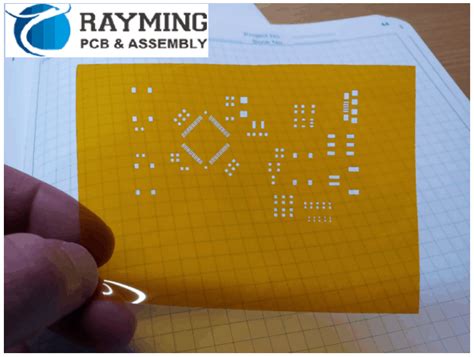
Solder stencils, also known as solder paste stencils, are thin metal sheets with cutouts that match the pads on a printed circuit board (PCB). They are used to apply solder paste onto the PCB pads in a precise and controlled manner before components are placed and the board is sent through a reflow oven for soldering.
Solder stencils play a crucial role in the surface mount technology (SMT) assembly process. They ensure that the right amount of solder paste is deposited onto each pad, leading to reliable solder joints and a high-quality finished product.
Key Benefits of Using Solder Stencils
-
Precision: Solder stencils allow for accurate and consistent solder paste deposition, ensuring that each pad receives the appropriate amount of solder.
-
Efficiency: Using solder stencils significantly speeds up the SMT Assembly process compared to manual solder paste application.
-
Repeatability: Solder stencils enable the production of multiple identical PCBs with consistent solder paste application.
-
Versatility: Solder stencils can be used with a wide range of PCB designs and component packages, from small chip components to large BGAs.
Types of Solder Stencils
There are several types of solder stencils available, each with its own advantages and limitations.
Laser-Cut Stencils
Laser-cut stencils are made by using a high-powered laser to cut the apertures into a thin sheet of stainless steel. They offer several benefits:
- High precision and accuracy
- Quick turnaround times
- Ability to create fine pitch apertures
- Suitable for prototyping and low-volume production
However, laser-cut stencils can be more expensive than other types and may have limitations on the minimum aperture size and spacing.
Chemical-etched Stencils
Chemical-etched stencils are created by selectively etching away material from a stainless steel sheet using a chemical process. They offer the following advantages:
- Lower cost compared to laser-cut stencils
- Ability to create larger apertures
- Suitable for high-volume production
However, chemical-etched stencils may have lower precision and accuracy compared to laser-cut stencils, and the etching process can be time-consuming.
Electroformed Stencils
Electroformed stencils are made by electroplating nickel onto a photoresist-patterned master. They provide several benefits:
- Excellent surface finish and aperture definition
- Ability to create very fine pitch apertures
- High durability and long lifespan
However, electroformed stencils are generally more expensive than other types and have longer lead times.
| Stencil Type | Advantages | Limitations |
|---|---|---|
| Laser-cut | High precision, quick turnaround, fine pitch | Higher cost, minimum aperture size restrictions |
| Chemical-etched | Lower cost, larger apertures, high-volume | Lower precision, time-consuming process |
| Electroformed | Excellent finish, fine pitch, high durability | Higher cost, longer lead times |

Designing Solder Stencils
Proper solder stencil design is essential for achieving reliable solder joints and a high-quality PCB Assembly. Here are some key factors to consider when designing solder stencils:
Aperture Size and Shape
The aperture size and shape should be optimized based on the component package and PCB pad design. Generally, the aperture should be slightly larger than the pad to allow for proper solder paste release. Common aperture shapes include:
- Square: Used for most SMD pads
- Round: Used for circular pads, such as those found on BGA packages
- Oblong: Used for rectangular pads or to compensate for misalignment
Stencil Thickness
The stencil thickness determines the amount of solder paste deposited onto the pads. Thicker stencils deposit more solder paste, while thinner stencils deposit less. The optimal stencil thickness depends on factors such as the component package, pad size, and desired solder joint profile.
Common stencil thicknesses range from 0.004″ (0.1 mm) to 0.01″ (0.25 mm), with 0.006″ (0.15 mm) being a popular choice for many applications.
Aperture Orientation and Spacing
Aperture orientation and spacing should be carefully considered to ensure proper solder paste release and to minimize bridging between adjacent pads. Some guidelines to follow include:
- Orienting apertures at 45° to the squeegee direction to improve paste release
- Providing sufficient spacing between apertures to prevent bridging
- Avoiding apertures that are too close to the edge of the stencil
Fiducial Marks
Fiducial marks are used to align the solder stencil with the PCB during the stencil printing process. They should be included in the stencil design and placed in locations that are easily visible and accessible by the stencil printer’s vision system.

Solder Paste Selection
Choosing the right solder paste is crucial for achieving high-quality solder joints and reliable PCB assembly. Some factors to consider when selecting solder paste include:
- Alloy composition: Common alloys include SAC305 (Sn96.5/Ag3.0/Cu0.5) and Sn63/Pb37
- Particle size: Smaller particle sizes are better for fine-pitch components, while larger particle sizes are suitable for larger components
- Flux type: No-clean, water-soluble, and rosin-based fluxes are available, each with its own advantages and limitations
- Viscosity: The solder paste’s viscosity should be suitable for the stencil thickness and aperture size
| Alloy | Melting Point (°C) | Composition |
|---|---|---|
| SAC305 | 217-220 | Sn96.5/Ag3.0/Cu0.5 |
| Sn63/Pb37 | 183 | Sn63/Pb37 |
| Sn42/Bi57.6 | 138 | Sn42/Bi57.6 |
| Indalloy 1 | 118 | In50/Sn50 |

Solder Paste Printing Process
The solder paste printing process involves the following steps:
- Aligning the solder stencil with the PCB using fiducial marks
- Applying solder paste to the stencil surface
- Using a squeegee to spread the solder paste across the stencil, forcing it through the apertures and onto the PCB pads
- Lifting the stencil away from the PCB, leaving the solder paste deposits on the pads
- Inspecting the solder paste deposits for consistency and accuracy
To ensure a successful solder paste printing process, consider the following factors:
- Squeegee pressure: Adjust the pressure to achieve proper solder paste release without damaging the stencil or PCB
- Squeegee speed: Optimize the speed to ensure complete filling of apertures and consistent solder paste deposits
- Separation speed: Control the speed at which the stencil is lifted away from the PCB to prevent solder paste from sticking to the stencil
- Print direction: Alternate the print direction (forward and backward) to minimize solder paste buildup on the stencil
Stencil Cleaning and Maintenance
Regular cleaning and maintenance of solder stencils are essential for ensuring consistent solder paste printing results and extending the stencil’s lifespan. Some best practices include:
- Cleaning the stencil after every print cycle using a lint-free wipe and a suitable cleaning solution
- Periodically performing a thorough cleaning using an ultrasonic cleaner to remove dried solder paste and debris
- Inspecting the stencil for damage, wear, or clogged apertures and repairing or replacing as necessary
- Storing the stencil in a clean, dry environment to prevent contamination and damage
Troubleshooting Common Solder Paste Printing Issues
Despite careful design and process control, issues can still arise during solder paste printing. Here are some common problems and their potential solutions:
-
Insufficient solder paste deposit: Increase stencil thickness, enlarge aperture size, or adjust squeegee pressure and speed.
-
Excessive solder paste deposit: Decrease stencil thickness, reduce aperture size, or adjust squeegee pressure and speed.
-
Solder paste bridging: Increase spacing between apertures, reduce stencil thickness, or optimize squeegee pressure and speed.
-
Poor solder paste release: Clean or replace the stencil, adjust aperture design, or optimize separation speed.
-
Inconsistent solder paste deposits: Check for stencil damage or wear, ensure proper alignment, and maintain consistent process parameters.
| Issue | Potential Solutions |
|---|---|
| Insufficient paste deposit | Increase thickness, enlarge apertures, adjust pressure/speed |
| Excessive paste deposit | Decrease thickness, reduce apertures, adjust pressure/speed |
| Solder paste bridging | Increase spacing, reduce thickness, optimize pressure/speed |
| Poor paste release | Clean/replace stencil, adjust apertures, optimize separation speed |
| Inconsistent deposits | Check stencil condition, ensure alignment, maintain consistency |
FAQ
1. How often should I clean my solder stencil?
It is recommended to clean your solder stencil after every print cycle using a lint-free wipe and a suitable cleaning solution. Additionally, perform a thorough cleaning using an ultrasonic cleaner periodically to remove dried solder paste and debris.
2. What factors affect the solder paste deposit volume?
Several factors can affect the solder paste deposit volume, including:
- Stencil thickness
- Aperture size and shape
- Squeegee pressure and speed
- Solder paste viscosity and particle size
3. How do I prevent solder paste bridging between pads?
To prevent solder paste bridging, consider the following:
- Increase the spacing between apertures
- Reduce the stencil thickness
- Optimize the squeegee pressure and speed
- Ensure proper stencil alignment and cleanliness
4. Can I reuse a solder stencil after a long storage period?
Yes, you can reuse a solder stencil after a long storage period, provided that it has been stored properly in a clean, dry environment and is free from damage or contamination. Before using the stencil, clean it thoroughly and inspect it for any signs of wear or damage.
5. How do I choose the right solder paste for my application?
When selecting a solder paste, consider the following factors:
- Alloy composition: Choose an alloy that is compatible with your PCB and components, and meets your performance requirements.
- Particle size: Select a particle size that is appropriate for your component pitch and stencil aperture sizes.
- Flux type: Consider the cleaning requirements, environmental factors, and performance needs when choosing a flux type (no-clean, water-soluble, or rosin-based).
- Viscosity: Ensure that the solder paste viscosity is suitable for your stencil thickness and aperture sizes, and that it provides good printability and tackiness.
Consult with your solder paste supplier or manufacturer for guidance on selecting the best solder paste for your specific application.
In conclusion, solder paste stencils play a crucial role in the SMT assembly process, ensuring accurate and consistent solder paste deposition for reliable solder joints. By understanding the types of stencils available, designing stencils properly, selecting the right solder paste, and optimizing the printing process, you can achieve high-quality PCB assemblies with minimal defects. Regular stencil maintenance and troubleshooting skills are also essential for maintaining consistent results and prolonging the life of your solder stencils.


Leave a Reply