Understanding HDI PCB Cost Drivers
To effectively reduce HDI PCB costs, it is essential to understand the factors that contribute to the overall expense. Some of the primary cost drivers include:
- Material selection
- Layer count and board thickness
- Via structure and density
- Surface finish
- Manufacturing process complexity
By addressing these factors and making informed decisions, it is possible to optimize costs while maintaining the desired performance and reliability.
Strategies for HDI PCB Cost Reduction
Optimize Layer Count and Board Thickness
One of the most significant factors affecting HDI PCB costs is the number of layers and the overall board thickness. To reduce costs, consider the following:
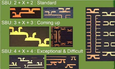
- Minimize the number of layers by efficiently routing traces and utilizing advanced design techniques, such as blind and Buried vias.
- Opt for thinner base materials, such as 1.6mm or 1.2mm, when possible to reduce material costs and improve signal integrity.
- Use a combination of standard and HDI layers to balance cost and performance.
| Layer Count | Cost Impact |
|---|---|
| 4 | Low |
| 6 | Medium |
| 8 | High |
| 10+ | Very High |
Optimize Via Structure and Density
Via structure and density play a crucial role in HDI PCB costs. Consider the following strategies to reduce via-related expenses:
- Minimize the number of blind and buried vias, as they require additional drilling and plating processes.
- Use microvias only when necessary, and consider stacked or staggered via arrangements to reduce drilling costs.
- Employ via-in-pad technology to save space and reduce layer count.
| Via Type | Cost Impact |
|---|---|
| Through | Low |
| Blind | Medium |
| Buried | High |
| Stacked | High |
| Staggered | Medium |
Select Cost-Effective Materials
Material selection has a direct impact on HDI PCB costs. To reduce expenses, consider the following:
- Choose lower-cost base materials, such as FR-4, when the application allows.
- Opt for standard copper weights, such as 0.5oz or 1oz, to avoid additional processing costs.
- Use cost-effective surface finishes, such as ENIG or OSP, when appropriate.
| Material | Cost Impact |
|---|---|
| FR-4 | Low |
| High Tg | Medium |
| Polyimide | High |
| Rogers | High |
Optimize Manufacturing Processes
Streamlining the manufacturing process can help reduce HDI PCB costs. Consider the following strategies:
- Design for manufacturability (DFM) to minimize production challenges and reduce the risk of defects.
- Use standard panel sizes and layouts to optimize material usage and reduce waste.
- Collaborate with your PCB manufacturer to identify cost-saving opportunities and ensure design feasibility.
Leverage Economies of Scale
Increasing production volume can significantly reduce the per-unit cost of HDI PCBs. Consider the following:
- Consolidate multiple designs into a single panel to reduce setup and tooling costs.
- Place larger orders to benefit from volume discounts offered by PCB manufacturers.
- Establish long-term partnerships with suppliers to negotiate better pricing and ensure a stable supply chain.

Balancing Cost and Quality
While reducing HDI PCB costs is important, it is crucial to maintain the desired level of quality and reliability. To achieve this balance, consider the following:
- Prioritize cost reduction strategies that have minimal impact on performance and reliability.
- Conduct thorough testing and validation to ensure the HDI PCBs meet the required specifications.
- Monitor supplier performance and quality metrics to identify potential issues and take corrective action.

Case Studies
Company A: Automotive Electronics Manufacturer
Company A, a leading automotive electronics manufacturer, successfully reduced HDI PCB costs by 25% without sacrificing quality. They achieved this by:
- Optimizing layer count and board thickness
- Minimizing the use of blind and buried vias
- Selecting cost-effective materials and surface finishes
- Collaborating with their PCB manufacturer to streamline the production process
As a result, Company A maintained their competitive edge in the market while improving their bottom line.
Company B: Consumer Electronics Startup
Company B, a consumer electronics startup, faced the challenge of reducing HDI PCB costs to meet their tight budget constraints. They implemented the following strategies:
- Leveraging economies of scale by consolidating multiple designs into a single panel
- Using a combination of standard and HDI layers to balance cost and performance
- Optimizing via structure and density
- Establishing a partnership with a reliable PCB manufacturer
Through these efforts, Company B successfully reduced their HDI PCB costs by 35% while ensuring the quality and performance of their products.

Frequently Asked Questions (FAQ)
-
Q: What is the difference between HDI PCBs and traditional PCBs?
A: HDI PCBs have higher component density and use advanced manufacturing techniques, such as blind and buried vias, to accommodate complex designs. Traditional PCBs have lower component density and primarily use through-hole vias. -
Q: Can I use cheaper materials for HDI PCBs to reduce costs?
A: While using cheaper materials can reduce costs, it is essential to ensure that the selected materials meet the performance and reliability requirements of the application. Always consider the balance between cost and quality when making material choices. -
Q: How can I determine the optimal layer count for my HDI PCB Design?
A: The optimal layer count depends on factors such as the complexity of the design, signal integrity requirements, and cost constraints. Collaborate with your PCB manufacturer and use design tools to determine the most cost-effective layer count that meets your performance needs. -
Q: Is it always necessary to use blind and buried vias in HDI PCBs?
A: Blind and buried vias are often used in HDI PCBs to accommodate high component density and complex routing requirements. However, they also increase manufacturing costs. Consider using blind and buried vias only when necessary and explore alternative routing strategies to minimize their use. -
Q: How can I ensure the quality of my HDI PCBs while reducing costs?
A: To ensure quality while reducing costs, focus on design for manufacturability (DFM), select reliable suppliers, and conduct thorough testing and validation. Establish clear quality metrics and monitor supplier performance to identify and address any issues promptly.
Conclusion
Reducing HDI PCB costs without sacrificing quality is achievable through a combination of strategic design decisions, material selection, process optimization, and collaboration with reliable manufacturing partners. By understanding the cost drivers and implementing the strategies discussed in this article, companies can effectively reduce HDI PCB expenses while maintaining the desired level of performance and reliability.
As the demand for high-density electronics continues to grow, the ability to optimize HDI PCB costs will remain a critical factor in maintaining a competitive edge in the market. By staying informed about the latest cost reduction techniques and working closely with experienced PCB manufacturers, companies can successfully navigate the challenges of balancing cost and quality in HDI PCB production.


Leave a Reply