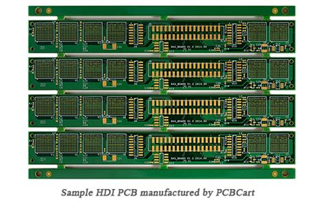
Introduction to HDI PCBs
High Density Interconnect (HDI) Printed Circuit Boards (PCBs) are advanced circuit boards that offer higher component density and improved electrical performance compared to traditional PCBs. HDI PCBs are characterized by their fine line widths, small via sizes, and high layer counts, enabling the miniaturization of electronic devices while maintaining or enhancing functionality.
In today’s rapidly evolving electronics industry, HDI PCBs have become increasingly popular due to their ability to accommodate complex designs and meet the demands of modern, high-performance applications. This article will delve into the structure, manufacturing process, and benefits of HDI PCBs.
Key Features of HDI PCBs
HDI PCBs are distinguished by several key features that set them apart from conventional PCBs:
-
Fine line widths and spacing: HDI PCBs typically have trace widths and spacing of 3 mils (0.075 mm) or less, allowing for higher routing density and more compact designs.
-
Microvias: These are small, laser-drilled vias with diameters of 6 mils (0.15 mm) or less. Microvias enable interconnections between layers without consuming valuable board space.
-
High layer counts: HDI PCBs often have 8 or more layers, providing increased routing options and allowing for more complex designs.
-
Blind and Buried vias: These vias connect inner layers without being visible on the surface of the board, further increasing routing density and design flexibility.
-
Thin substrates: HDI PCBs use thinner substrate materials, such as polyimide or liquid crystal polymer (LCP), to reduce overall Board Thickness and improve electrical performance.

HDI PCB Structure
The structure of an HDI PCB consists of several key components:
1. Substrate Material
The substrate is the foundation of the PCB, providing mechanical support and electrical insulation. Common substrate materials for HDI PCBs include:
- FR-4: A glass-reinforced epoxy laminate, FR-4 is the most widely used substrate material for PCBs due to its good mechanical and electrical properties, as well as its cost-effectiveness.
- Polyimide: This high-performance polymer offers excellent thermal stability, mechanical strength, and electrical insulation, making it suitable for demanding applications.
- Liquid Crystal Polymer (LCP): LCP is a high-performance thermoplastic with low dielectric constant and loss, high thermal stability, and excellent moisture resistance, making it ideal for high-frequency applications.
2. Copper Layers
HDI PCBs typically have multiple copper layers, ranging from 4 to 16 or more. These layers are used for signal routing, power distribution, and grounding. The copper layers are laminated together with the substrate material and interconnected through vias.
3. Solder Mask
The solder mask is a protective coating applied to the outer layers of the PCB. It serves to insulate the copper traces, prevent solder bridging, and provide a surface for component labeling. Solder masks are typically green, but other colors are available for specific applications.
4. Silkscreen
The silkscreen is a printed layer on top of the solder mask that provides component identifiers, polarity markers, and other important information for assembly and maintenance. Silkscreen is usually white, but other colors can be used for better visibility or aesthetics.
5. Surface Finish
The surface finish is applied to the exposed copper pads to protect them from oxidation and enhance solderability. Common surface finishes for HDI PCBs include:
- Electroless Nickel Immersion Gold (ENIG): A layer of nickel is plated onto the copper, followed by a thin layer of gold. ENIG provides excellent solderability, durability, and shelf life.
- Immersion Silver (IAg): A thin layer of silver is chemically deposited onto the copper. IAg offers good solderability and is a cost-effective alternative to ENIG.
- Organic Solderability Preservative (OSP): A thin, organic coating is applied to the copper to protect it from oxidation. OSP is a cost-effective option but has a limited shelf life compared to metallic finishes.

HDI PCB Manufacturing Process
The manufacturing process for HDI PCBs involves several critical steps:
1. Design and Layout
The first step in HDI PCB manufacturing is the design and layout of the circuit. This involves creating a schematic diagram, selecting components, and designing the physical layout of the board using computer-aided design (CAD) software. The layout must adhere to the design rules and constraints specific to HDI PCBs, such as minimum trace widths, via sizes, and clearances.
2. Material Selection and Preparation
Once the design is finalized, the appropriate substrate material is selected based on the application requirements. The substrate is then cut to the desired size and shape, and any necessary pre-treatment, such as cleaning or surface conditioning, is performed.
3. Lamination
The substrate layers, along with the copper foils, are stacked and aligned according to the design. The stack is then subjected to high temperature and pressure in a lamination press, bonding the layers together to form a solid, multilayer board.
4. Drilling
After lamination, the board undergoes drilling to create through-holes and vias. For HDI PCBs, laser drilling is commonly used to create microvias, as it offers high precision and the ability to create smaller, more closely spaced vias compared to mechanical drilling.
5. Plating
The drilled board is then plated with copper to create electrical connections between layers. This is typically done using electroless copper plating, followed by electrolytic copper plating to achieve the desired thickness.
6. Patterning
The copper-plated board is then patterned to create the desired circuit layout. This involves applying a photoresist coating, exposing it to UV light through a photomask, and developing the resist to reveal the desired pattern. The exposed copper is then etched away, leaving only the desired traces and pads.
7. Solder Mask Application
A solder mask is applied to the board to protect the copper traces and prevent solder bridging. The solder mask is typically applied using a screen printing or photoimaging process, and then cured to harden the coating.
8. Surface Finish Application
The chosen surface finish is applied to the exposed copper pads to protect them from oxidation and enhance solderability. The application method depends on the specific surface finish, but common methods include immersion plating, electroless plating, and hot air solder leveling (HASL).
9. Silkscreen Printing
The silkscreen layer is printed onto the board using a screen printing process. This layer provides component identifiers, polarity markers, and other important information for assembly and maintenance.
10. Electrical Testing
Finally, the completed HDI PCB undergoes electrical testing to ensure that it meets the desired specifications and performance requirements. This may include continuity testing, insulation resistance testing, and high-potential (hipot) testing.

Benefits of HDI PCBs
HDI PCBs offer several significant benefits over traditional PCBs:
-
Miniaturization: The high component density and fine feature sizes of HDI PCBs enable the creation of smaller, more compact electronic devices.
-
Improved electrical performance: The shorter signal paths and reduced parasitic capacitance and inductance of HDI PCBs result in better signal integrity and higher-speed operation.
-
Increased functionality: The higher layer counts and routing density of HDI PCBs allow for more complex designs and increased functionality within a given board size.
-
Reduced weight: The use of thinner substrates and the overall reduction in board size contribute to lighter-weight electronic devices.
-
Cost-effectiveness: Although HDI PCBs may have higher initial costs compared to traditional PCBs, their ability to accommodate more complex designs and reduce overall system size can lead to cost savings in the long run.
Applications of HDI PCBs
HDI PCBs find applications in a wide range of industries and products, including:
- Consumer electronics: Smartphones, tablets, laptops, and wearable devices.
- Telecommunications: 5G infrastructure, network equipment, and wireless devices.
- Automotive: Advanced driver assistance systems (ADAS), infotainment systems, and vehicle connectivity modules.
- Medical devices: Implantable devices, diagnostic equipment, and medical imaging systems.
- Aerospace and defense: Avionics, satellite systems, and military communication devices.
- Industrial automation: Robotics, process control systems, and IoT devices.
Challenges and Considerations
While HDI PCBs offer numerous benefits, there are also some challenges and considerations to keep in mind:
-
Design complexity: HDI PCB designs are more complex and require specialized knowledge and tools. Designers must be familiar with the specific design rules and constraints associated with HDI PCBs.
-
Manufacturing challenges: The smaller feature sizes and tighter tolerances of HDI PCBs require advanced manufacturing capabilities and stricter process control. Not all PCB manufacturers may have the necessary equipment and expertise to produce HDI PCBs reliably.
-
Material selection: The choice of substrate material and surface finish can significantly impact the performance and reliability of HDI PCBs. Designers must carefully consider the application requirements and environmental factors when selecting materials.
-
Testing and inspection: The high density and small features of HDI PCBs can make testing and inspection more challenging. Specialized equipment and techniques, such as 3D x-ray inspection and automated optical inspection (AOI), may be necessary to ensure quality and reliability.
-
Cost: HDI PCBs typically have higher initial costs compared to traditional PCBs due to the advanced materials, manufacturing processes, and testing requirements. However, the long-term cost savings from miniaturization and improved performance can often justify the investment.
Frequently Asked Questions (FAQs)
-
Q: What is the difference between HDI PCBs and traditional PCBs?
A: HDI PCBs have finer feature sizes, higher component density, and more layers compared to traditional PCBs. This enables the creation of smaller, more complex, and higher-performance electronic devices. -
Q: What are microvias, and why are they important in HDI PCBs?
A: Microvias are small, laser-drilled vias with diameters of 6 mils (0.15 mm) or less. They enable interconnections between layers without consuming valuable board space, allowing for higher routing density and more compact designs. -
Q: What materials are commonly used for HDI PCB substrates?
A: Common substrate materials for HDI PCBs include FR-4, polyimide, and liquid crystal polymer (LCP). The choice of material depends on the specific application requirements, such as thermal stability, electrical performance, and cost. -
Q: How do HDI PCBs improve electrical performance compared to traditional PCBs?
A: HDI PCBs have shorter signal paths and reduced parasitic capacitance and inductance due to their finer feature sizes and higher component density. This results in better signal integrity and higher-speed operation. -
Q: What industries and applications commonly use HDI PCBs?
A: HDI PCBs are widely used in industries such as consumer electronics, telecommunications, automotive, medical devices, aerospace, and defense. They are particularly suited for applications that require miniaturization, high performance, and increased functionality.
Conclusion
HDI PCBs represent a significant advancement in printed circuit board technology, offering numerous benefits over traditional PCBs. Their fine feature sizes, high component density, and improved electrical performance enable the creation of smaller, more complex, and higher-performance electronic devices.
The manufacturing process for HDI PCBs involves several critical steps, from design and layout to material selection, lamination, drilling, plating, patterning, and testing. Each step requires specialized knowledge, tools, and processes to ensure the quality and reliability of the final product.
While HDI PCBs present some challenges, such as design complexity, manufacturing requirements, and higher initial costs, their long-term benefits often justify the investment. As electronic devices continue to evolve and demand more advanced capabilities, HDI PCBs will play an increasingly important role in shaping the future of the electronics industry.


Leave a Reply