Introduction to Flexible PCBs
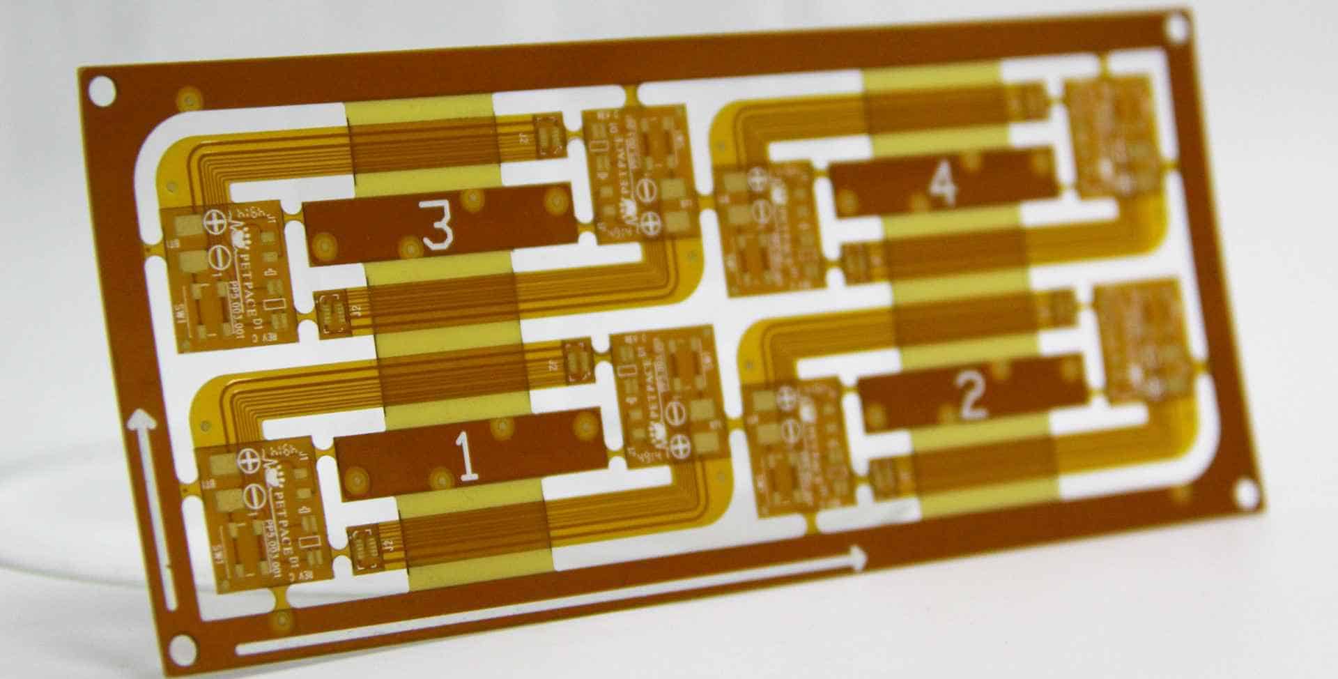
Flexible printed circuit boards (flex PCBs) are a type of printed circuit board made with flexible base material like polyimide film instead of traditional rigid fiberglass. This allows the PCB to bend and flex while still maintaining electrical connectivity. Flex PCBs were first developed in the 1960s for use in aerospace applications, but today they are used in a wide variety of consumer and industrial electronics where flexibility, space savings, or vibration resistance are required. Some common applications of flexible PCBs include:
- Wearable devices
- Medical devices
- Robotics and drones
- Foldable/rollable displays
- Automotive electronics
Compared to rigid PCBs, flex PCBs provide a number of advantages:
- Can conform to different shapes and spaces
- Lightweight and thin
- Vibration and impact resistant
- Allows for movable parts and connections
- Easier to install and prototype
- Often lower costs at higher production volumes
However, there are also some limitations to consider:
- Less thermal dissipation without a rigid board
- Generally fewer layers and complexity than rigid PCBs
- May require special connectors or mounts
- More challenging assembly process
As the applications for flex PCBs continue to grow, it’s important for design engineers to understand the specialized design and manufacturing considerations when working with flex PCBs.
Flexible PCB Materials
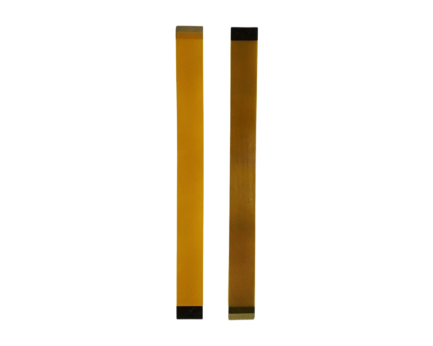
The base material for flex PCBs is a flexible dielectric film such as polyimide (Kapton), polyester (PET), or PEN. Polyimide is the most common type of film used. It has excellent thermal stability and chemical resistance while maintaining flexibility. The most widely known brand of polyimide film is DuPont’s Kapton film.
The conductive layers on a flex PCB are typically very thin copper foil, ranging from 1/2 oz (17 μm) to 2 oz (70 μm) in thickness. This allows the copper to flex along with the base film. A thin layer of adhesive bonds the copper foil to the base film.
There are two main types of flexible circuit materials:
Single Sided Flex – A basic flex PCB with conductive traces on only one side of the base film.
Double Sided Flex – Flexible circuit with conductive layers on both sides of the dielectric film. Allows for higher trace densities.
Some high density or multilayer flex PCBs may also use rigid boards such as FR-4 strategically placed in certain areas while retaining flexibililty in other parts of the circuit.
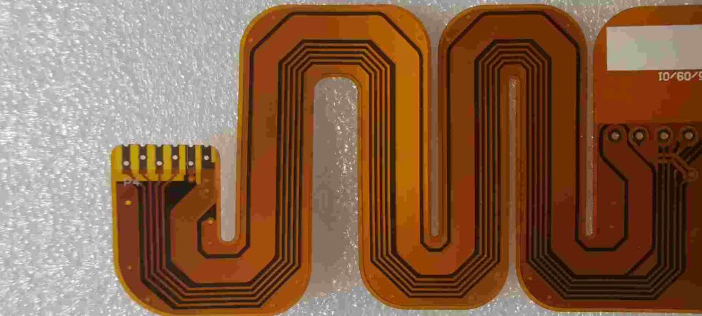
Flex PCB Design Rules
Designing a flex PCB requires following specialized design rules to ensure the circuit can flex repeatedly without failure. Here are some of the most important flex PCB design guidelines to consider:
- Trace width – Traces should be at least 6 mils (0.15mm) wide to ensure adequate conductivity for most applications. High current carrying traces may need to be wider.
- Trace spacing – A minimum of 3-5 mils spacing should be used between traces for common voltages. Higher spacing for traces with greater voltage differences.
- Bending radius – Avoid sharp bends. Bend radii should be at least 2-3 times the board thickness.
- Stiffeners – Adding stiffeners made of rigid material around connectors or components prevents damage from flexing in those areas.
- Adhesives – Use flexible adhesives like polyurethane that can withstand bending. Avoid brittle adhesives.
- Vias – Use staggered microvias instead of through hole vias which can crack under bending forces.
- Annular rings – Pads should have larger annular rings (6-8 mil) to prevent tearing.
- Component placements – Strategically place components in areas of the PCB that will not bend or on rigid islands.
Properly designing flex PCBs requires specialized CAD tools and an understanding of flex design requirements.
Flex PCB Manufacturing Process Overview
While flexible PCB manufacturing uses some of the same principles as rigid PCB fabrication, it requires some additional specialized processes and equipment to handle the flexible base material. Here is a simplified overview of the flex PCB fabrication process:
1. Base Material Preparation
The flexible dielectric film is cleaned, cut to size, and prepared for metallization. Films like polyimide may require special pretreatments.
2. Metallization
The base film is coated with an ultra-thin layer of copper foil using a metallization process like sputtering or electroless plating.
3. Photolithography
A photoresist is applied over the copper layer and then exposed to UV light through a mask. The exposed photoresist is washed away.
4. Etching
The unexposed copper is etched away, leaving behind the desired conductive copper traces.
5. Dielectric Bonding
Adhesive dielectric layers are applied between layers of circuitry to provide insulation. Multilayer flex circuits require stacked laminated layers.
6. Drilling
Microvias are drilled through the dielectric layers to interconnect layers. Precise laser drilling avoids cracking flexible films.
7. Plating and Coating
Exposed copper traces are plated with metals to protect against corrosion and improve solderability. Solder mask, coverlay, and other coatings are applied as needed.
8. Testing and Finishing
The finished flex PCBs are electrically tested. Final finishes like covercoat, carbon printing, or EMI shielding are applied as needed. Singulation divides panels into individual PCBs.
Flex PCB fabrication provides several advantages over rigid PCB manufacturing. The flexible base films are easier to work with and enable roll-to-roll processing for many fabrication steps like metallization, improving productivity. The additive processes used also generate less hazardous chemical waste.
Selecting a Flexible PCB Manufacturer
Choosing the right flex PCB manufacturer is crucial for getting high quality, reliable circuits produced. Here are some key things to look for when selecting a flex PCB production partner:
- Experience – Look for manufacturers with expertise specifically in flex PCB fabrication, not just rigid boards. They should have extensive knowledge of flex materials, design, and manufacturing processes.
- Qualifications – Leading manufacturers will have certifications like ISO 9001 for quality management and ISO 14001 for environmental practices. Some may also have industry specific qualifications like certification for medical or aerospace applications.
- Capabilities – Ensure they can support all the features you need like multilayer, high density interconnects, blind vias, etc. Discuss your specific project requirements in detail.
- Volume production – If high volume manufacturing is required, seek companies with capacity for longer production runs of 1,000+ units. They should have automated equipment tailored for high output.
- Prototyping – For early stage prototyping and shorter runs below 1,000 units, find providers focused on fast turnaround of prototypes and small batches.
- Quality control – Rigorously test sample boards to validate production quality before full manufacturing runs. Review their quality assurance procedures as well.
- Materials – Confirm they have experience with the necessary base materials like polyimide films for your application requirements.
- Communication – Responsiveness and technical expertise when discussing your application requirements are positive signs of a strong partner.
Taking the time to properly evaluate and select your flex PCB manufacturing partner will pay off with shorter development cycles and reliable performance.
Cost Factors in Flexible PCB Manufacturing
When budgeting for your flexible PCB project, there are a number of factors that influence the overall costs:
- Board size – Base material costs will be higher for larger board dimensions. Typical panels range from 200-400mm.
- Layer count – Each additional conductive layer adds cost for materials, processes like lamination, and lower yields. 2-6 layers are typical.
- Features – More complex features like high density interconnects, buried vias, blind/filled vias, etc. drive up fabrication costs.
- Tolerances – Tighter tolerances on traces and spacing require more careful processes. Looser tolerances are cheaper.
- Flexibility – More bend cycles drive up base material quality and processing requirements. Rigid-flex costs more than pure flex.
- Testing – Extensive electrical testing, AOI inspection, and other quality assurances increase costs but reduce long term issues.
- Volume – Small batch prototyping has high setup costs per board. Larger production runs distribute costs over more boards.
- Lead time – Rush delivery times often incur higher costs for expedited fabrication. Standard lead times are cheaper.
Discussing your budget constraints and cost drivers with your manufacturer early on allows them to find the most cost-effective fabrication process to meet your needs.
Applications of Flexible Printed Circuits
Some of the industries and products taking advantage of flexible PCB technology include:
Wearable Devices – Fitness trackers, smart watches, health monitors, and other wearables use thin, light flex circuits that can conform to the human body.
Medical Devices – Hearing aids, pacemakers, patient monitors, and other medical electronics rely on flex PCBs for biocompatibility, reliability, and space savings.
Automotive – Around 20-30 flex PCBs are used per car for engine controls, dashboard displays, sensors, lighting, anti-lock brake systems, and other applications.
Robotics – Flexible circuits allow movement for joints and limbs in robotics and machinery while maintaining necessary connections.
Aerospace – Flex PCBs withstand vibration while minimizing weight in guidance systems, engine controls, antennas, and other avionics applications.
Displays – LCD, OLED, and touch screen displays are moving to flex PCB backplanes as screens become foldable and curved.
Consumer Electronics – Cameras, mobile devices, and other portable electronics take advantage of durable, lightweight flex circuits.
As electronics become more compact, portable, and flexible, demand for flex PCBs will continue rising across nearly every industry.
Future Developments in Flexible Circuits
Some emerging areas of innovation in flex PCB technology include:
- Stretchable electronics – Materials and fabrication methods that allow flex PCBs to stretch and deform well beyond traditional capabilities.
- Biocompatible circuits – Flexible materials and coatings tailored for medical and implantable uses.
- Additive manufacturing – Printed electronics techniques like inkjet and aerosol printing can deposit conductive traces onto flex substrates.
- High frequency applications – Novel dielectric materials and fabrication techniques to enable flex PCBs for high frequency applications like 5G antennas.
- Thin, multilayer flex – Continued improvements in fine line patterning and stacked lamination to produce very thin but multilayer flex circuits.
- 3D shaped circuits – Flexible circuits that can take on 3D shapes rather than lying flat, providing design freedom.
- Rigid-flex integration – Tighter integration of rigid board sections and components into flexible circuits to take advantage of both technologies.
With R&D expanding the possibilities for flex PCBs, designers have more options than ever to take advantage of flexible circuit boards in their electronics.
Frequently Asked Questions About Flex PCBs
What are some typical design guidelines for flex PCBs?
Some key flex PCB design guidelines include trace widths of at least 6 mils, trace spacing of 3-5 mils minimum, bend radii at least 2-3x the board thickness, large annular rings around pads, strategic placement of components and stiffeners, and use of flexible adhesives.
How many times can a flex PCB be flexed before failing?
Most robust flex PCB materials like polyimide films can withstand hundreds of thousands to millions of dynamic flex cycles before traces may start to crack or lift from the substrate, depending on the bend radius.
How small can traces and spacing be done on flexible circuits?
The finest line width and spacing is driven by the copper thickness and manufacturing capabilities, but traces down to 3-4 mil with 3-4 mil spacing are typical for high density flex PCBs. Finer geometries are possible for some applications.
Can components be mounted directly to flexible PCBs?
Yes, components can be surface mounted but the soldering process requires care. Alternatively, rigid islands can be used to provide stability for mounting components while retaining flexibility elsewhere.
How are vias created on flex PCBs?
Microvias drilled with lasers are used instead of through-holes. Staggered or filled vias avoid ripping of flexible base films while allowing layer transitions.
Conclusion
Flexible printed circuit boards provide invaluable advantages for electronics that need to bend, flex, or conform to unique spaces. As PCBs move beyond traditional rigid boards, it is essential for design engineers to understand the specialized processes involved in flex PCB fabrication. By following proper design guidelines, selecting qualified manufacturers, and leveraging the benefits of flex circuits, engineers can take advantage of flex PCB technology for all sorts of cutting edge, compact devices.


Leave a Reply