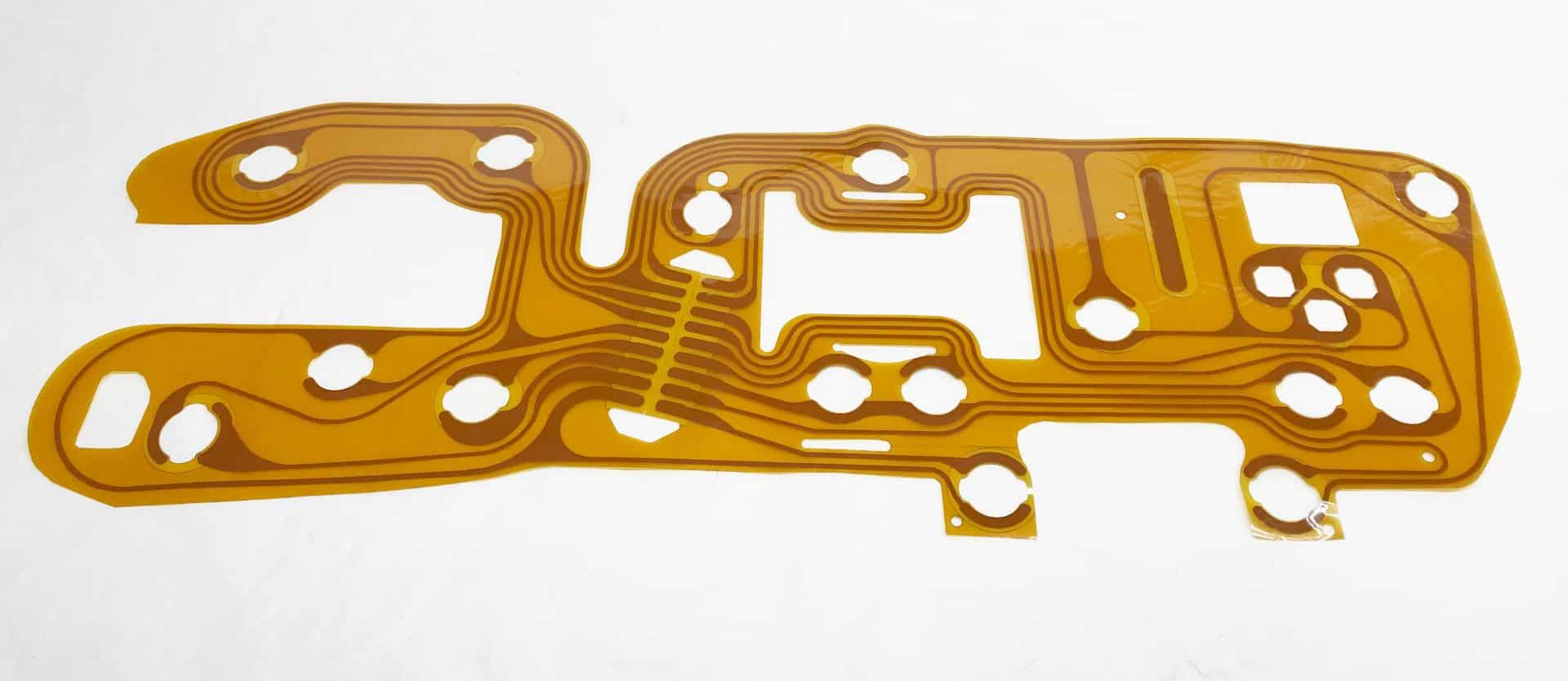
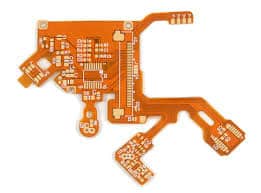
Flexible printed circuit boards (flex PCBs) are a type of printed circuit board made with flexible substrate materials such as polyimide and polyester. Flex PCBs can be bent, folded, and twisted to fit into tight spaces and movable configurations. They are commonly used in consumer electronics, medical devices, automotive electronics, and aerospace applications where flexibility and space constraints are important design considerations.
Flex PCBs provide several advantages over rigid PCBs:
- They can conform to 3D shapes and enable flexible form factors for devices
- They allow dynamic flexing and repeated bending during use
- They are lightweight and have a thin profile
- They can connect moving parts within an assembly
However, flex PCB fabrication also poses some unique challenges compared to rigid PCB manufacturing. This article provides an overview of the flex PCB manufacturing process, design considerations, and benefits of using a professional flex PCB manufacturer.
Flex PCB Manufacturing Process Overview
The basic steps in manufacturing a flex PCB include:
- Design and layout
- Material selection
- Photolithography
- Etching
- Silkscreen printing
- Lamination
- Electrical testing
- Singulation
- Final assembly
The design, photolithography, etching, lamination, and testing steps have similarities to rigid PCB fabrication. However, there are some differences in the materials used, specialized techniques required, and additional process considerations needed for flex PCBs.
Flex PCB Design
The design of a flex PCB requires special considerations compared to a rigid board:
- Trace widths and spaces are generally larger to accommodate flexing
- Avoidance of 90 degree angles and use of curved traces instead
- Minimizing components and vias on the flexing areas
- Accounting for dynamic flex zone folding and bending
Most flex PCBs use a single-sided or double-sided trace layout, with more layers possible but less common. The CAD software also needs to support the import of mechanical outlines for the flexing zones.
Material Selection
The substrate material for flex PCBs is a flexible dielectric film such as polyimide or polyester. The most common thickness range is 12.5 to 125 microns. Polyimide provides better heat resistance while polyester is more economical.
The conductive traces are typically made from rolled annealed copper foil, with a thickness of around 18 to 35 microns. Some applications require silver plated traces for improved conductivity or gold plating for corrosion resistance.
Cover layers consist of an acrylic-based solder mask and ink-based or UV-cured legend printing. Stiffeners made from materials like aluminum or polyimide film can be selectively added to reinforce certain areas.
Photolithography
The trace patterns are formed on the flex substrate through a photolithography process, similar to rigid PCB fabrication. An LPI (liquid photoimageable) solder mask is coated over the bare copper foil. The solder mask is then exposed to UV light through a phototool, and the uncured areas are chemically washed away.
The remaining cured solder mask acts as an etch resist to protect the underlying copper during etching. The uncovered copper is selectively removed to create the circuit pattern.
Etching
There are a few etching methods used in flex PCB production:
- Wet chemical etching – The most common method, uses solutions like ammonium persulfate or ferric chloride to dissolve the unprotected copper
- Laser etching – A CO2 laser ablates away the unwanted copper instead of chemicals
- Plasma etching – Uses ionized gas plasma to etch away copper not covered by solder mask
Wet etching requires extra chemicals and disposal considerations, but provides higher throughput. Laser etching is slower but more environmentally friendly.
Lamination
Unlike rigid boards, flex PCBs require a lamination step to bond the layers together. The process involves aligning the substrate, adhesive sheets, and copper foil layers on a press bed. The materials are laminated together under pressure around 175-300 psi while heated to 180-200°C.
The combination of heat, pressure, and adhesive resin creates a strong permanent bond. Multi-layer flex PCBs undergo repeated lamination cycles to build up the required number of layers.
Electrical Testing
Electrical testing verifies the integrity of the flex PCB traces, vias, connections, and insulation. Testing methods include:
- Flying probe testing to check shorts/opens
- ICT (in-circuit testing) for assessing assembled boards
- Functional testing of input/output signals
- AOI (automated optical inspection) to examine trace defects
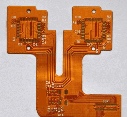
Assembly and Connectors
Common component assembly methods for flex PCBs are soldering, conductive epoxy adhesive, and mechanical connections. Care must be taken during soldering to avoid excessive heat damage.
Mating connectors and crimped terminals are attached to enable connections to components, cables, or rigid PCBs. Stiffeners may be added to provide structural support and minimize flexing at connector joints.
Benefits of Professional Flex PCB Manufacturing
While it’s possible to produce basic flex PCBs in lower volumes using in-house etching methods, working with a professional flex PCB manufacturer provides many advantages:
- Experience with specialized flex fabrication techniques and machinery
- Consistent quality and reliability
- Rigorous quality control at every manufacturing stage
- Large production capacity for higher volumes
- DFM analysis to optimize designs for manufacturability
- Testing services to validate PCB function
- Inventory management and procurement of specialized flex materials
- Seamless order fulfillment and logistics pipeline
- Support for quick-turn prototypes in addition to production quantities
This expertise and infrastructure allow flex PCB fabricators to handle complex multi-layer designs with fine features and challenging technical requirements. They serve customers across many industries and offer robust solutions tailored to the application.
Benefits of Flex PCB Technology
Beyond the manufacturing considerations, adopting flex PCB technology provides many benefits for product developers:
- Conformability to tight spaces and moving joints
- Lightweight, thin, and compact electronics packaging
- Improved reliability compared to wired harness assemblies
- Dynamic flexing capability for millions of cycles
- Simplified assembly by integrating interconnections
- Enhanced industrial design flexibility and aesthetics
- Miniaturization of products through tight integration
- Cost savings versus complex mechanical solutions
- Support for automated mass production
The demand for flex PCBs is experiencing strong growth as designers seek to integrate more functionality into smaller products. Their unique characteristics make flex circuits well-suited for the needs of wearable devices, IoT sensors, driverless vehicles, AR/VR systems, robotic systems, and other emerging applications.
Flex vs Rigid-Flex PCBs
There is some confusion between pure flex PCBs and rigid-flex boards. The main differences are:
- Flex PCB – Made entirely from thin, flexible dielectric substrate material and do not contain any rigid sections. Designed for dynamic flexing applications.
- Rigid-flex PCB – Multi-part boards with both rigid and flexible substrates combined in one assembly. The rigid sections provide mechanical support while the flex portions interconnect between them. Used in applications requiring both rigid support and flexible connections.
Hybrid rigid-flex boards provide more structure but also increase manufacturing complexity compared to pure flex circuits. Both technologies serve important roles depending on the mechanical design constraints and freedom of movement required.
Flex PCB Materials
As explained above in the manufacturing process overview, the main materials used in flex PCB fabrication include:
- Base Substrate – Polyimide, polyester, PEEK, and LCP films in 12.5 to 125 micron thickness range. Polyimide is most common.
- Conductive Traces – Rolled annealed copper foil, typically with 18 to 35 micron thickness. May be plated with immersion silver, immersion tin, or gold.
- Bonding Adhesive – Acrylic or epoxy adhesive films like Pyralux and epoxy are used to bond layers together.
- Coverlay – Liquid photoimageable solder mask, dry film solder mask, or flex coverlay to protect conductors.
- Stiffeners – Additional polyimide, aluminum, or FR4 layers in certain areas to provide mechanical rigidity.
- Legend Ink – Ink-based inks and UV-cured inks are used for silkscreen printed component legends and board markings.
Comparison of Flex PCB and Rigid PCB Attributes
| Attribute | Flex PCB | Rigid PCB |
|---|---|---|
| Substrate material | Polyimide, polyester, fluoropolymer films | FR-4 glass reinforced epoxy |
| Layer count | Typically 1 or 2 layer. Up to 12 layers possible. | Up to >50 layers |
| Minimum trace/space | 125 um / 125 um | 125 um / 125 um |
| Bend radius | Flexible, dynamic high cycle bends | Fixed shape, only limited bends |
| Components | Requires special packaging, no BGAs | SMT components, BGAs, connectors |
| Vias | Limited number, tenting required | Large number of vias |
| Thermal issues | Poor thermal conductivity | Can dissipate heat efficiently |
| Cost | Generally higher | Lower in high volumes |
| Lead time | Longer | Shorter |
| Applications | Dynamic flexing, constrained spaces | High density interconnections |
Factors That Influence Flex PCB Cost
The cost of a flex PCB depends on many variables in the design, specifications, materials, and manufacturing process factors:
- Board size – Measured in square inches. Larger boards have higher material costs.
- Layer count – Single sided lowest cost. Each additional layer adds expense.
- Feature size – Fine line designs require tighter tolerances and precision.
- Flexibility – More bend cycles and tighter dynamic flexing increase cost.
- Stiffeners – Addition of stiffeners adds material expense.
- Adhesives – Specialized high-temp adhesive films are more costly.
- Solder mask – LPI solder masks are preferred but add expense over dry film.
- Plating – Gold over copper tracing is more expensive than tin/lead plating.
- Volume – Prototypes in low volume are more expensive per board.
- Lead time – Rush turnaround times increase costs.
- Testing/QC – Extensive electrical testing and inspection adds cost.
- Certifications – Rigorous quality management standards like ISO 9001 lead to higher overhead expenses.
By working closely with a flex PCB manufacturer during the design phase, engineers can optimize the cost while still meeting all essential electrical, mechanical, and reliability requirements.
Flex PCB Design Guideline Examples
Here are some example flex PCB design guidelines to follow:
- Minimize component concentration on dynamic flexing areas
- Avoid 90 degree angles on traces, use rounded curves instead
- Place components in periodic arrays for even distribution of stress
- Use teardrop pads at junctions between conductors and pads
- Allow 5X copper thickness spacing between conductors
- Allow 3X polyimide thickness spacing for flexible dielectric gaps
- Limit panelization transport vias around tooling holes
- Verify minimum bend radius for flex zones
- Include fiducials for assembly alignment
- Eliminate stiffeners and copper planes from high flex areas
- Distribute heat-generating components for thermal dissipation
- Reduce unnecessary tracings beneath components
- Utilize stress relief perforations in the polyimide film if needed
These guidelines help improve the flex PCB performance, avoid failures like fractured traces, and support the requirements for repeated dynamic bending cycles.
Applications and Examples of Flex PCBs
Flex PCBs are used in a wide range of applications across many industries:
Consumer Electronics
- Wearable devices (smart watches, fitness trackers)
- Laptop and tablet computer flex interconnects
- Foldable mobile phones and devices
- Digital camera modules and gimbal assemblies
- VR/AR headsets
Automotive Use Cases
- Automotive camera interconnects
- Seat heaters and sensors
- Flex antennas
- Tire pressure monitoring sensors
- Blind spot detection sensors
- Powertrain sensors
Medical Devices
- Hearing aids
- Blood glucose monitors
- Endoscopes
- Catheters
- Ultrasound transducers
- Implantable devices
Industrial
- Robotics flex cabling
- Nano-satellites in aerospace
- Oil/gas downhole drilling sensors
- High temperature sensors
Military/Defense
- Missile guidance systems
- Radar and antenna arrays
- Soldier-worn systems
This range of use cases illustrates the versatility of flex PCB technology across markets that require compact, lightweight, and movable electronics.
Key Takeaways on Flex PCB Manufacturing
Some of the key points about flex PCB fabrication include:
- Flex PCBs allow dynamic bending and folding compared to rigid boards
- Polyimide and polyester films used as base substrate materials
- Rolled annealed copper with 18-35um thickness for traces
- Photolithography and etching create the conductor pattern
- Polymer composite adhesive films bond the layers
- Must withstand repeated flexing cycles without failure
- Used in applications with tight space constraints and moving joints
- Professional flex PCB manufacturers offer expertise, quality, and testing services
- Flex PCBs enable innovative designs but require design considerations for flex zones
- Cost depends on size, layer count, features, flex requirements, and materials
Flexible Printed Circuit Board (FPCB) Manufacturing FAQ
Here are some frequently asked questions about flex PCB manufacturing:
Q: What are the most commonly used materials for flex PCB fabrication?
A: The most common substrate materials are polyimide and polyester films. Other materials like PEEK or LCP films are used for high temp flex applications. Copper foil is most widely used for the conductive traces.
Q: What are some key differences when designing a flex PCB versus a rigid PCB?
A: Flex PCB designs require larger features, avoidance of 90 degree angles, evenly distributed components, minimized traces under components, and additional clearances between conductors in the flex zones.
Q: What are some examples of components that can be assembled on flex PCBs?
A: Typical component types are SMT passives, LEDs, connectors, sensors, and simple ICs in either packaged or bare die form. BGA packages are not suitable for flex PCB assembly.
Q: How many layers can modern flex PCBs support?
A: While 1 or 2 layers are most common, advanced flex PCBs can incorporate up to 12 layers, allowing more complex circuit designs.
Q: What testing is performed to ensure a quality flex PCB?
A: Testing involves visual inspection at multiple stages as well as electrical testing like flying probe, functional test, and ICT. This ensures the design integrity and flexing performance meet requirements.
So in summary, working with an experienced flex PCB manufacturer and following design guidelines tailored for dynamic flex zones are key to successfully implementing a flex PCB assembly into your product. Flex circuits enable innovative form factors not possible with rigid boards alone.


Leave a Reply