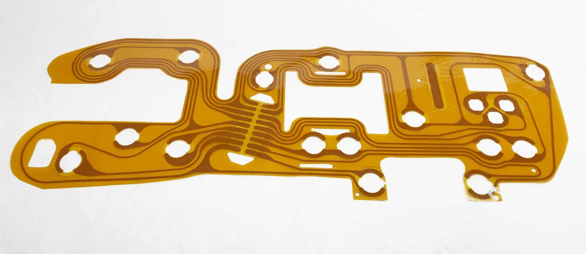
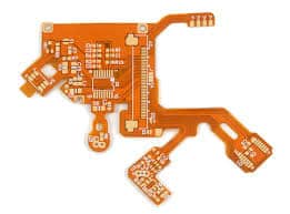
Introduction to Flex PCBs
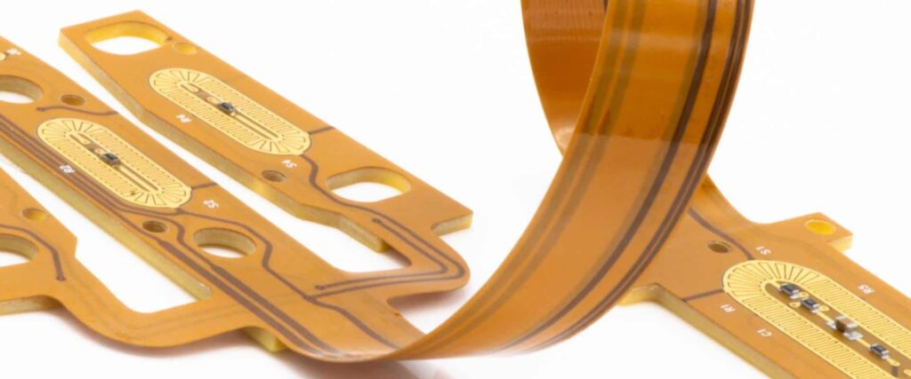
A flex PCB, also known as a flexible printed circuit board, is a type of PCB that can bend and flex. Flex PCBs are made from flexible materials like polyimide instead of rigid materials like FR4. This allows them to be folded, twisted, and shaped to fit into tight spaces in products like mobile phones, wearables, medical devices, and more.
Flex PCBs provide several advantages over rigid PCBs:
- Dynamic flexing – They can move and flex with other components during use. This helps prevent damage from vibration or impact.
- Space savings – Their thin profile lets them fit into tight spaces where rigid PCBs won’t work.
- Weight reduction – Flex PCBs weigh less than rigid versions. This helps make end products lighter.
- Reliability – The flexible material and traces resist cracking better than rigid boards.
- Design freedom – Flex PCBs allow for more creative, efficient, and compact product designs.
Flex PCB Layer Stacks
The layer stack refers to the number of conductive copper layers and dielectric material layers in a PCB. Flex PCB stacks tend to be simpler than rigid PCB stacks. Here are some common flex layer stack configurations:
Single Layer Flex PCB
A single layer (1 layer) flex PCB has one layer of copper traces on a flexible dielectric substrate. The minimum bend radius is very small. Simple wiring and low density connections are suitable for single layer flex PCBs.
Two Layer Flex PCB
A two layer (2 layer) flex PCB adds another layer of copper traces to a single layer flex PCB. One layer is on the bottom and one layer is on the top. The layers are separated by a flexible dielectric material. Two layer flex PCBs support moderate wiring density and complexity.
Multilayer Flex PCB
Multilayer flex PCBs have three or more layers of circuitry separated by flexible dielectric layers. This allows for increased wiring density and more complex circuit designs. Typical layer counts are 4, 6, and 8 layers. The more layers used, the higher the flex PCB cost and minimum bend radius.
Flex Stackup: Cover Layers
In addition to the copper and dielectric layers that make up the functional circuitry, flex PCBs also have cover layer materials on the outer surfaces. These cover layers protect the flex PCB and components mounted on it.
Coverlay
A coverlay is a thin, flexible dielectric layer laminated onto the top and/or bottom of the flex circuit. Coverlay protects the traces from damage and prevents electrical shorts. Common coverlay materials include polyimide, acrylic, and epoxy.
Stiffener
Some flex PCBs have a stiffener material applied to all or part of the flex circuit. The stiffener makes that section of the PCB more rigid to aid in component mounting. Stiffeners can be polyimide, acrylic, or metal like aluminum or stainless steel.
Choosing a Flex PCB Layer Stack
Here are some guidelines on selecting the right layer stack for your flex PCB design:
- Use the fewest number of layers possible to reduce costs and maximize bend radius.
- Choose a stackup based on your circuit complexity and connection density needs.
- Add cover layers like coverlay or stiffeners in areas that need extra protection or rigidity.
- Consult with your flex PCB manufacturer if unsure about material selection and stackup.
- Prototype with basic 2 layer flex PCBs first before committing to more complex multilayer stacks.
- Perform bend tests to ensure the layer stack can flex enough for your application.
- Carefully consider how traces will cross between layers and use vias appropriately.
Flex PCB Layer Fabrication and Testing
Professional flex PCB manufacturers use specialized processes to fabricate the layer stack:
Layer Alignment
Aligning the layers precisely is critical to ensure traces match up across layers. This is done using lamination jigs and vision alignment systems.
Bond Enhancement
Chemical or mechanical surface treatments help the flexible layers bond tightly during lamination. This prevents delamination.
Registration
Photos or x-rays of the layer alignment are used to check registration of the layers. This verifies they are aligned correctly.
AOI Inspection
Automated optical inspection (AOI) examines the flex PCB for defects between layers like misregistration or opens.
Cross-section
Cross-sectioning cuts a sample flex PCB layer stack in half so the alignment can be inspected under a microscope.
Flex Durability Testing
Test flex PCB samples are stressed through repeated bending, twisting, and folding to ensure the traces and layers do not crack.
Flex PCB Layer Stack Design Rules
Here are some key design rules to follow when laying out your flex PCB layer stack:
- Maintain at least 0.1mm trace spacing between conductors on a layer
- Use larger trace widths for high current paths to prevent overheating
- Minimize the number of layers to cross signals for simpler layout
- Use vias to transition traces between layers where needed
- Avoid putting vias in bend areas to prevent damage
- Limit component density in flexing areas to prevent damage from repeated stresses
- Use generous bend radius sizes of at least 3-5X the total board thickness
- Add stiffeners and cover layers in high stress component areas
- Minimize conductor lengths running along the neutral axis to reduce flex cracks
Flex PCB Layer Stack Examples
Here are some examples of different products using various flex PCB layer stack configurations:
Wearable Devices
Wearables like smart watches often use simple 1 or 2 layer flex PCBs. The thin stacks can dynamically flex during use without much impact on size.
Medical Electronics
Medical devices need rigid sections for connectors and components along with flexible sections for dynamic cabling. Selective stiffeners help create these rigid zones.
Robotics and UAVs
Robots and drones may embed flex PCBs throughout the mechanical structures. Multilayer flex with at least 4-6 layers often provides sufficient wiring density.
Consumer Gadgets
Phones, laptops, and game systems need dense cabling in tight spaces. High layer count flex PCBs with 6-8 layers help interconnect components.
Conclusion
Understanding flex PCB layer stacks is important for designing durable and reliable flex circuits. The number of layers, cover layers, minimum bend radius, trace spacing, and other factors must be considered carefully based on the application. Working with an experienced flex PCB manufacturer ensures your design is fabricated correctly. With the right flex layer stack design, you can create compact and innovative products.
FQA
What are the main advantages of using a flex PCB?
Some key advantages of flex PCBs over rigid PCBs are:
- Dynamic flexing to prevent damage from motion
- Thin profile to fit into tight spaces
- Lightweight and portable
- Increased reliability and durability
- More design freedom and efficiency
How many layers are typical for most flex PCB designs?
Simple flex PCBs usually have 1 or 2 layers. Intermediate complexity designs often use 4-6 layers. High density flex circuits may have 8+ layers but this increases cost and bend radius. 2 and 4 layer stacks are suitable for many applications.
What cover layer materials are commonly used?
Polyimide film and acrylic are two popular coverlay materials to protect flex PCB outer layers. Adhesives bond the coverlay. Stiffeners made from polyimide or metal provide rigidity. Cover layers protect traces and aid mounting.
What fabrication processes help ensure proper layer alignment?
Precision lamination jigs and vision alignment systems properly position the flex PCB layers. Registration and microscopy inspect alignment. Testing verifies the layers withstand repeated flexing without cracking.
How can stiffeners and coverlays help make a flex PCB more robust?
Stiffeners applied to areas with connectors or tightly spaced components make those regions more rigid for stability. Coverlayers over all the traces protect the entire flex PCB from scratches and shorts. This improves durability.


Leave a Reply