Introduction
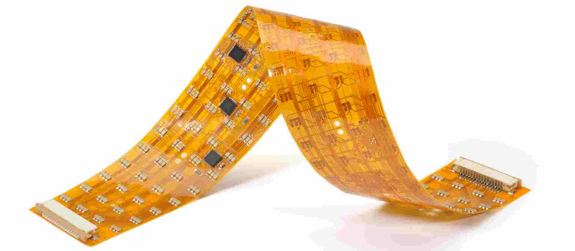
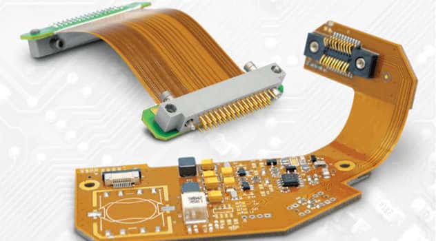
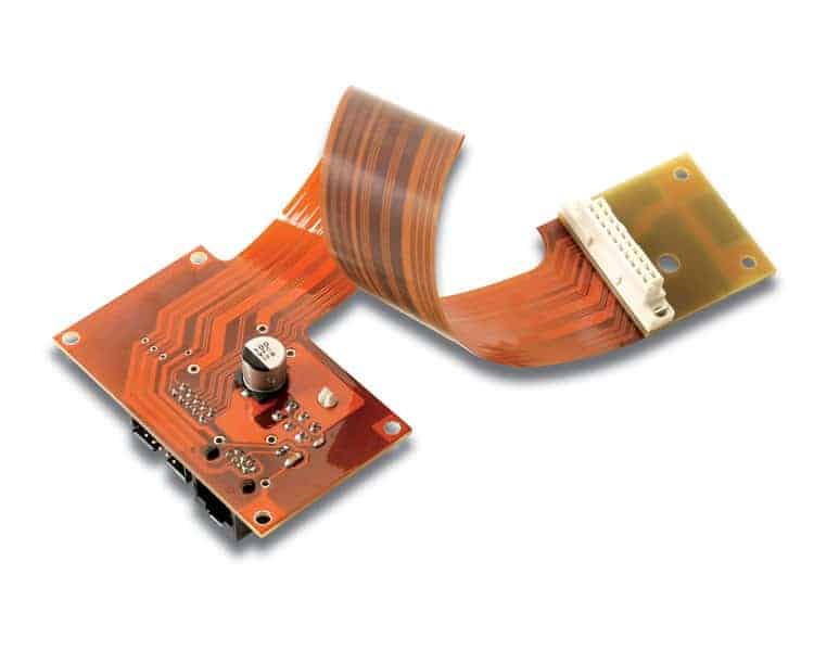
A flexible printed circuit board (flex PCB) is a technology that allows circuits to be assembled on flexible and bendable substrates. Flex PCBs provide several advantages over traditional rigid PCBs such as reduced weight, space savings, improved reliability and the ability to conform to dynamic surfaces.
As flex PCB technology has matured, it has been increasingly adopted across a wide range of industries and applications including consumer electronics, automotive, medical devices, aerospace, and more. With the growth in flex PCB usage, understanding the specialized flex PCB fabrication process has become crucial for design engineers and manufacturers alike.
This comprehensive guide covers the key aspects of the flex PCB fabrication process including materials, design considerations, manufacturing steps, testing and quality control. By the end of this article, readers will have a complete overview of the end-to-end process flow for manufacturing high-quality flex PCBs.
Flex PCB Materials
Flex PCBs begin with the selection of appropriate base materials that can provide the needed electrical, mechanical and thermal performance. Some key material considerations are covered below:
Substrates
The flexible substrate is the foundation upon which flex PCB circuits are built. The most commonly used substrates are polyimide (Kapton) and polyester (PET) films ranging from 12.5 to 100 microns in thickness. In general, polyimide provides superior thermal performance and polyester offers better economy. Some key substrate properties are:
- Dielectric strength
- Thermal capabilities
- Chemical resistance
- Dimensional stability
- Flexibility
Conductors
Conductive traces are made up of metallic foils like copper laminated onto the flexible substrate. Common foil thicknesses range from 12.5 to 50 microns. Selecting the right thickness depends on current carrying needs and bending radius requirements.
Coverlayers
Coverlayers or covercoats are insulating films that are laminated over the top of a processed flex PCB to prevent shorting between conductors. Polyimide is most commonly used due to its thermal endurance, flexibility and durability. Coverlayers typically range from 12.5 to 50 microns in thickness.
Adhesives
Adhesives are used to bond the different layers together. Acrylic, epoxy and polyimide are some common adhesives used in flex PCBs. Factors like bond strength, flexibility and heat resistance are considered during adhesive selection.
Flex PCB Design Guidelines
Careful design is crucial for flex PCBs in order to account for their unique mechanical and electrical properties during use. Some key flex PCB design guidelines include:
- Minimum trace widths and spacing: Conductors on flex circuits need increased spacing due to potential dynamic flexing during use. Typical trace/space is 5 mil (0.127mm) line/5 mil space.
- Coverlayer openings: Openings in coverlayers need rounded corners instead of sharp corners to prevent tearing.
- Bend radius: Traces should not be routed across inside bend areas. Minimum bend radius rules prevent damage.
- Stiffeners: Rigid stiffeners, usually polyimide films, are often added in heavily populated sections to prevent damage.
- Adhesives: Proper adhesive selection can help control flexing in targeted areas of the PCB.
- Vias: Use stacked or filled vias instead of through-hole vias for reliability in dynamic bending apps.
- Test Points: Include test/probe points to account for lack of access to flexing PCB sections during testing.
Flex PCB Fabrication Process Steps
The specialized materials and properties of flex PCBs require unique fabrication processes tailored to flex boards. The figure below shows a typical multi-layer flex PCB fabrication workflow.<img src=”https://i.postimg.cc/BLYWwRH3/Flex-PCB-Process.png” width=”100%” style = “margin-bottom:20px;”>
The key steps in the flex PCB fabrication process are:
1. Materials Preparation
The base substrate material is cut to size and holes are punched based on assembly needs. For multi-layer flex boards, adhesive coated bondply layers and prepreg dielectric layers are also prepared.
2. Metal Foil Lamination
Copper foils are laminated onto the substrate along with any adhesive coated dielectric layers using high heat and pressure in a vacuum press. This bonds the materials together into a rigid board.
3. Photolithography
A photosensitive dry film is laminated onto the PCB and then exposed to UV light through a mask. This transfers the circuit image pattern onto the PCB.
4. Etching
The PCB is etched in chemical solutions to remove exposed copper and leave behind the desired circuit traces protected by the photoresist.
5. Photoresist Stripping
The remaining dry film photoresist is then stripped away leaving behind the finished copper circuitry.
6. Dielectric Layer Lamination
For multilayer flex PCBs, additional layers are stacked using adhesive coated dielectric prepreg layers. The layers are precisely aligned and then laminated together.
7. Via Formation
Mechanical drilling or laser ablation is used to form vertical interconnect vias through the dielectric layers. The vias are then plated to form electrical connections between layers.
8. Outerlayer Processing
Steps 3 to 5 are repeated to form circuits on the external layers of the PCB stackup. This completes the flex PCB fabrication.
9. Solder Mask
A solder mask layer is applied to coat the entire flex PCB providing insulation and preventing solder bridging. Clear areas are defined for soldering.
10. Finishing
The flex PCB panels go through a battery of finishing processes including hole plugging, bevelling, electrical testing, and more.
11. Assembly
After fabrication, components are assembled onto the flex PCB using soldering or adhesive methods to produce the final populated circuit.
Flex PCB Testing
Key test equipment used includes optical microscopes, x-ray inspection tools, flying probe testers and automated optical inspection (AOI) systems.
Flex PCB Quality Control
To ensure consistent quality and reliability, flex PCB manufacturers follow stringent quality control procedures:
- Statistical process control to minimize process variability
- Regular machine and tool calibration
- Traceability systems for materials, equipment and personnel
- Environmental controls for temperature, humidity and contamination
- Certifications such as ISO 9001 to standardize processes
- First article inspections for new designs
- Inline quality control checks at each process stage
- Quality training programs for employees
- Reliability testing like HAST, thermal cycling and vibration
By leveraging robust quality systems and inspection processes, manufacturers can achieve zero-defect flex PCB production.
Benefits of Working with a Flex PCB Partner
Partnering with an experienced flex PCB manufacturer provides many benefits:
- Flex Expertise: Take advantage of specialized flex PCB knowledge for design, materials, fabrication and assembly.
- Quality: Ensure rigorous quality control standards are met for high reliability flex circuits.
- Cost Savings: Pooling volume allows access to economies of scale and cost optimizations.
- Lead Times: Avoid capacity bottlenecks through flex PCB partners with production flexibility.
- One-Stop Solution: Work with a partner that provides complete services from prototyping to volume production.
- Continuous Improvement: Leverage regular process upgrades at flex PCB production facilities.
- Global Footprint: Use flex PCB partners with facilities close to your supply chain needs.
Conclusion
As flex PCB technology enables smaller, faster and more reliable electronics, understanding the nuances of flex fabrication becomes more important. This guide summarizes the specialized materials, design factors, manufacturing steps and quality processes involved in producing advanced flexible PCBs. By selecting the right flex PCB partner, product teams can stay focused on design while leveraging manufacturing experts for production. The result is high-performing flex PCBs that meet the demands of cutting-edge electronic devices.
Flex PCB Fabrication Frequently Asked Questions
1. What are some typical applications of flex PCBs?
Some common applications of flex PCBs include consumer electronics (laptops, mobile phones), automotive, aerospace, medical, robotics, wearables, IoT devices, and military equipment. The flexibility allows conforming to tight spaces and moving parts.
2. How do costs compare between rigid PCBs and flex PCBs?
Generally flex PCBs have higher cost per area compared to rigid PCBs. Key factors driving flex PCB costs higher are:
- Specialty flexible base materials
- More complex fabrication processing
- Lower volumes compared to rigid PCBs
- Advanced assembling challenges
However, the system-level benefits like reduced wiring, connectors and assembly costs should also be considered.
3. What are some methods used to assemble components onto flex PCBs?
Common assembly methods include:
- SMT: Surface mount assembly uses solder paste and reflow methods similar to rigid PCBs. This is suitable for flat flex areas.
- Soldering: Discrete through-hole components can be hand soldered or wave soldered.
- Conductive adhesive: Anisotropic conductive films or adhesive provide reliable interconnects.
- Mechanical attachment: Direct component attachments to flex PCB using screws, rivets or clips.
4. How are vias constructed in flex PCBs?
Common flex PCB via construction methods include:
- Stacked vias: Consist of pads on each layer interconnected by plated through holes. This provides the most reliable plating.
- Filled vias: Blind or buried vias are mechanically drilled and then filled with conductive ink or paste.
- Laser ablated: Excimer lasers can ablate microvias through flex dielectric layers. Plating forms connection.
5. What design factors should be considered for dynamic flex applications?
Some key considerations for dynamic flexing include:
- Analyze expected bending radii and setup appropriate rules.
- Use stacked or filled vias instead of drilled through hole vias.
- Avoid routing traces over bend areas.
- Use thick rolled annealed copper to improve flex life.
- Add stiffeners on heavily populated areas.
- Ensure adequate trace widths and clearances.
- Follow minimum pad sizes for plated through holes.
- Allow sufficient adhesive boundaries around flexing regions.


Leave a Reply