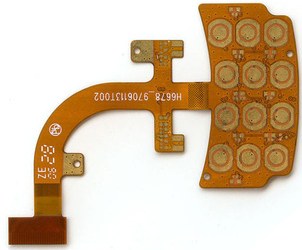
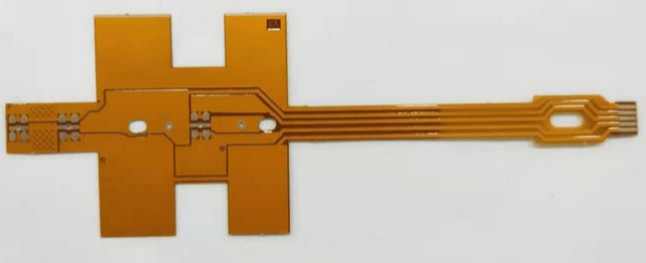
What is a Flex PCB?
A flexible printed circuit board (flex PCB) is a type of printed circuit board that can bend and flex. Flex PCBs are made from flexible materials like polyimide instead of rigid materials like FR-4. This allows the PCB to bend and move dynamically in tight spaces and complex form factors.
Flex PCBs are commonly used in small consumer electronics, medical devices, aerospace applications, and other products where flexibility and space savings are needed. Some key benefits of using a flex PCB include:
- Can fold and bend dynamically to fit complex shapes
- Thinner and lighter than rigid PCBs
- Allows movement and articulation of components
- Withstands vibration and flexing without damage
- Enables creative and compact product designs
- Can connect multiple rigid PCBs together
Design Considerations for Flex PCBs
When designing a flex PCB in Altium Designer, there are some important considerations:
Layer Stack
The layer stack for a flex PCB is different than a rigid PCB. Flex PCBs have flexible dielectric core layers like polyimide instead of rigid FR-4 layers. Common flex stackups include 1-4 metal layers with coverlay and adhesive layers. Ensure your stackup matches your manufacturing capabilities.
Minimum Bend Radius
Pay attention to the minimum bend radius supported by the flex material based on the number of layers. Tight folds can damage the tracks. Leave enough clearance for the radius under bending.
Stiffeners
Add stiffener materials or rigid sections in areas that do not require flexing. This helps avoid accidentally over-bending the PCB during use.
Vias
Use staggered or filled vias instead of simple drilled vias. This provides reliability under dynamic flexing. Filled vias withstand flexing better than open holes.
Trace Width/Spacing
Use larger trace widths and spacing than normal rigid PCBs. This helps reliability under bending and prevents thin traces from cracking.
Adhesives
Research adhesive options compatible with flex PCBs. Things like connectors will need adhesive anchoring. Select flexible and resilient adhesives.
Connectors
Use connectors designed for flex PCB applications. Look for types with flexible leads or solder anchors. Avoid connectors that could crack under bending.
Setting Up the Project in Altium
To start a new flex PCB project in Altium Designer:
- Open Altium Designer and select File > New > Project > PCB Project.
- Enter a project name and file location to save.
- In the New Project Wizard options, set the Default Board Type to Flex (Polyimide) Board.
- Set the Units to your desired measurement units – typically Milimeters.
- Choose the Number of Copper Layers based on your design needs.
- Select a Standard Board CutoutTemplate if needed, or setcustom dimensions.
- Set other parameters as desired like Fabrication Output andVersion Control.
- When ready, click Finish to create thenew flex PCB project.
This will setup an Altium project with a flexible PCB as the default board type. We can now configure the layer stack and design rules before starting board layout.
Configuring the Layer Stack
After creating the project, we need to define the layer stack. This involves picking the right flexible dielectric materials, defining the copper layers, and adding any coverlay or stiffeners.
To configure the layer stack:
- Open the Design > Layer Stack Manager.
- In the Layer Stack Manager, click the Add button.
- Select flexible materials like Polyimide for the Core layer type. Add the thickness.
- Add Copper layers. The copper thickness will be thinner than normal – typically around 1/3 to 1 oz.
- Repeat to add multiple polyimide core layers separated by copper signal layers.
- Use the Up/Down arrows to reorder the layers as needed.
- Add Coverlay layers on the top and bottom. Select coverlay materials and add the thickness.
- Define any internal plane layers or shielding layers if needed.
- Use the Preview pane to see a 3D view of the layer stack.
- When done, click OK to save the layer stack.
The layer stack is now configured for flex PCB fabrication. We can move on to setting design rules next.
Creating Flex Design Rules

Altium includes Flex design rule templates to help define common parameters like trace spacing and bend radius. We can start from these templates or create custom flex rules.
To setup design rules:
- Open the Design > Rules dialog.
- In the PCB Rules and Constraints tab, right-click and choose Add/Edit.
- In the constraints list, enable the Flex Design Rules. This adds pre-defined rules.
- You can edit any rule to change parameters like minimum trace width and spacing. Adjust values according to your flex material capabilities and design needs.
- Set the minimum bend radius rule. This is critical to prevent over bending the PCB during use.
- Apply any other standard PCB rules like routing widths, clearances, etc. Adjust values as needed.
- When done editing rules, click OK. The design rule check will now use these flex constraints.
The design rules will help guide the layout and validate the flex PCB design requirements. We can now start placing components and routing.
Placing Components and Routing
The general component placement and routing process is similar to normal PCB design in Altium. There are just a few additional things to consider for flex PCB layout:
- Component Anchoring – Use adhesive dots or polygons to anchor components that require additional holding force like connectors.
- Stiffening Sections – Add rigid sections or stiffeners made from materials like FR4 around components that can’t flex.
- Rounded Corners – Use teardrop tools when routing to round all trace corners. This prevents thin traces from cracking under bend stress.
- No 90 Degree Bends – Avoid routing traces at 90 degree angles. Use arcs or rounded angles when traces change direction on flex sections.
- Manage Slack – Carefully route out slack sections with generous bend radii where the PCB will dynamically flex. Avoid over constraining.
- Analyze Bends – Use the Flex Bend Analysis tool to validate minimum bend radius rules are satisfied.
Follow standard PCB layout practices taking these flex-specific guidelines into account. Make adjustments as needed during layout to optimize the flex design requirements.
Performing Design Rule Checks
Once all components are placed and routing is complete, be sure to run a thorough design rule check. The design rules defined earlier will validate the flex constraints like:
- Minimum bend radius
- Trace width/spacing
- Minimum flex layer distances
- Coverlay boundaries
- Acute trace angles
Carefully review any design rule violations that may require adjustments to the layout. Tuning the critical flex parameters during layout is important to achieving a successful and robust flex PCB design.
Generating Output Files
Like all PCB projects in Altium, we need to generate manufacturing output files to fabricate the board.
Some typical outputs needed for flex PCBs include:
- Gerber – Standard PCB fabrication layers
- ODB++ – Includes both gerber data and all layer stackup information
- Assembly Drawings – Help guide component placement and adhesive requirements
- 3D PDF – Allows interactive viewing of rigid-flex board assembly
- IPC-2581 – Alternative intelligent output file format
Use the Project > Generate Fabrication Outputs dialog in Altium to configure all needed manufacturing output files for your flex PCB design.
Summary
Designing a flex PCB requires following certain guidelines and constraints around the layer stack, trace routing, bend radius, and more. Altium Designer provides helpful tools like flex design rules, analysis features, and output generation specifically for flexible printed circuit boards.
With the right design approach, flex PCBs enable innovative solutions that would not be possible using only rigid boards. Following a robust design process in Altium helps ensure a successful flex PCB implementation.
FAQ
1. What type of connectors can be used on flex PCBs?
Special flex connectors are available with anchor tabs or flexible leads to withstand dynamic bending. Avoid rigid connectors not designed for flexing. Examples include FPC connectors, flex-tail connectors, and flex ribbon connectors.
2. Can components be mounted directly on the flex PCB?
Yes, but ensure components are properly anchored. Use adhesive dots, anchor pads, or polygons to hold parts that can’t flex. Avoid placing large or heavy SMT parts in highly dynamic areas.
3. What are some best practices for routing on flex PCBs?
Use rounded trace corners, avoid 90 degree bends, manage slack for flexing, use staggered vias, use larger trace widths, and perform bend analysis. Following flex routing constraints avoids cracking under dynamic bending.
4. How are multiple rigid and flex PCBs connected?
Rigid sections can be attached using board-to-board connectors on edges. Flex sections would fold to interconnect rigid sections. Ensure flex bend radius is compatible with any attached rigid boards.
5. Are there any special DFM considerations for flex PCBs?
Work closely with your flex PCB manufacturer on recommended design rules. Things like minimum trace spacing, bend radius, and coverlay tolerances depend on their specific flex materials and processes.


Leave a Reply