ALL ABOUT FLEX PCB
-
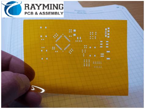
Making Solder Paste Stencils
Posted by
–
Read more: Making Solder Paste StencilsWhat are Solder Stencils? Solder stencils, also known as solder paste stencils, are thin metal sheets with cutouts that match the pads on a printed circuit board (PCB). They are used to apply solder paste onto the PCB pads in a precise and controlled manner before components are placed and […]
-
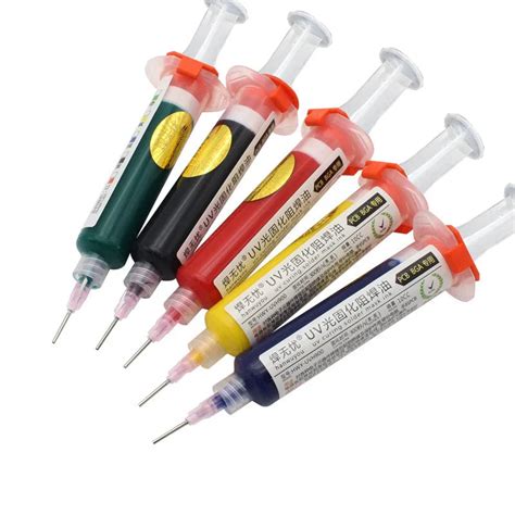
WHAT IS SOLDER MASK
Posted by
–
 Read more: WHAT IS SOLDER MASK
Introduction to Solder Mask Solder mask, also known as solder resist or solder stop, is a thin protective layer applied to the copper traces of a printed circuit board (PCB). This coating serves multiple purposes, including preventing solder bridges from forming between closely spaced solder pads, protecting the copper from […]
-
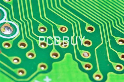
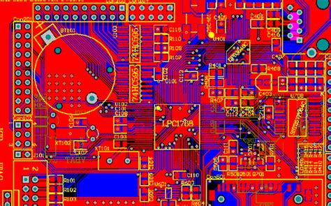
PCB Via Types
Posted by
–
 Read more: PCB Via Types
What Are PCB Vias? PCB vias are small holes drilled through a printed circuit board that allow electrical connections between different layers of the board. Vias are essential components in PCB Design as they enable compact and complex circuit routing in a limited space. By using vias, designers can create […]
-
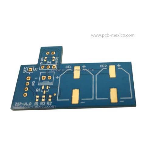
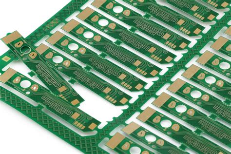
PCB manufacturer in Mexico
Posted by
–
 Read more: PCB manufacturer in Mexico
Introduction to PCB Manufacturing in Mexico Mexico has emerged as a prominent player in the global electronics industry, particularly in the manufacturing of printed circuit boards (PCBs). The country’s strategic location, skilled workforce, and favorable business environment have attracted numerous international companies to establish their PCB production facilities in Mexico. […]
-
 Read more: dimensions for panelization with breakaway tabs mouse bites
Understanding Panelization dimensions Panelization is a process in PCB manufacturing that involves grouping multiple printed circuit boards (PCBs) onto a single panel for efficient fabrication and assembly. This technique helps to reduce manufacturing costs, minimize handling, and optimize the use of materials. When designing panels for PCB production, it is […]
-
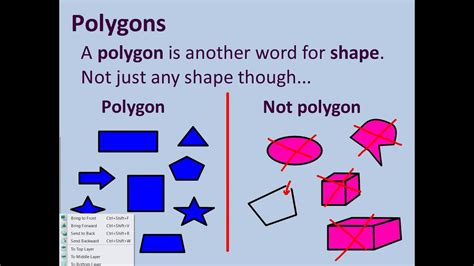 Read more: Altium Polygon pour breaks on rigid flex split lines
Understanding Polygon Pours in Altium Designer Polygon pours are a crucial feature in PCB design software like Altium Designer. They allow designers to fill large copper areas on the PCB with a solid connection to a specified net, providing low-impedance power distribution, shielding, and improved thermal management. However, when working […]
-
 Read more: HASL VS ENIG 10 Tips on How to Choose Enig Plating
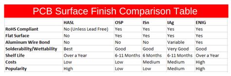
What is HASL? HASL is a surface finish that involves dipping the PCB into a molten solder bath and then using hot air to level the surface. This process creates a thin layer of solder on the exposed copper pads, providing protection against oxidation and ensuring good solderability. Advantages of […]
-
PCB File – What You Need To Know About
Posted by
–
 Read more: PCB File – What You Need To Know About
What is a PCB File? A PCB file, short for Printed Circuit Board file, is a digital file format used to store the design data for a printed circuit board. PCB files contain all the information needed to manufacture a physical PCB, including the board layout, component placement, routing, drill […]
-
What Is The Core Of A Custom Drone Board
Posted by
–
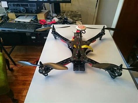 Read more: What Is The Core Of A Custom Drone Board
Main Components of a Custom Drone Board At the heart of any custom drone board are the following critical components: 1. Flight Controller Chip The flight controller is the main processor that runs the software and algorithms to keep the drone stable and flying as commanded. Some of the most […]
-
 Read more: 10 Differences Between HASL and ENIG Enig Plating Methods
What are HASL and ENIG Plating Methods? HASL (Hot Air Solder Leveling) and ENIG (Electroless Nickel Immersion Gold) are two common surface finish plating methods used in PCB manufacturing to protect exposed copper pads and provide a solderable surface. The choice between HASL vs ENIG depends on various factors such […]


