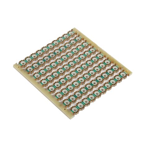
What is a Castellated PCB?
A castellated PCB (printed circuit board) is a type of circuit board that features plated holes or slots cut into the edges of the board. These castellations allow for easy and secure connections between multiple PCBs or modules without the need for external connectors or wires. The term “castellated” comes from the resemblance of these edge cuts to the battlements of a castle wall.
Castellated PCBs offer several advantages over traditional interconnection methods, making them an excellent choice for various electronic applications, especially those requiring modular designs or compact form factors.
Advantages of Using Castellated PCBs
1. Simplified Assembly Process
One of the primary benefits of using castellated PCBs is the simplified assembly process. With castellations, you can directly solder the modules together, eliminating the need for additional connectors or wires. This reduces the number of components required and streamlines the assembly process, saving time and cost.
2. Improved Mechanical Stability
Castellated connections provide improved mechanical stability compared to other interconnection methods. The plated holes or slots along the board edges create a strong and reliable bond between the modules when soldered together. This enhanced stability is particularly beneficial in applications that are subject to vibration, shock, or other mechanical stresses.
3. Reduced Space Requirements
By eliminating the need for external connectors, castellated PCBs allow for more compact designs. The modules can be placed closer together, reducing the overall footprint of the assembled board. This space-saving feature is crucial in applications where size constraints are a primary concern, such as wearable devices, IoT sensors, or compact electronic gadgets.
4. Enhanced Signal Integrity
Castellated connections can help maintain signal integrity by minimizing the distance between the interconnected modules. Shorter signal paths result in reduced parasitic inductance and capacitance, which can improve the performance of high-speed or high-frequency circuits. Additionally, the direct solder connections eliminate potential points of failure associated with external connectors, further enhancing signal reliability.
5. Cost-Effective Solution
Adopting castellated PCBs can lead to cost savings in various aspects of the manufacturing process. The simplified assembly process reduces labor costs, while the elimination of external connectors decreases the overall component count and associated expenses. Furthermore, the improved mechanical stability and signal integrity can result in higher yields and fewer field failures, ultimately reducing long-term costs.

Applications of Castellated PCBs
Castellated PCBs find applications in a wide range of industries and products, particularly those that benefit from modular designs or require compact form factors. Some common applications include:
- IoT Devices
- Wearable Electronics
- Aerospace and Defense Systems
- Automotive Electronics
- Medical Devices
- Consumer Electronics
- Industrial Control Systems
In each of these applications, castellated PCBs offer the advantages of simplified assembly, improved mechanical stability, reduced space requirements, enhanced signal integrity, and cost-effectiveness.

Designing Castellated PCBs
When designing castellated PCBs, several key considerations must be taken into account to ensure optimal performance and manufacturability.
1. Castellation Dimensions
The dimensions of the castellations, including the hole diameter, slot width, and edge clearance, should be carefully selected based on the specific requirements of the application. The hole diameter should be large enough to allow for reliable solder connections while considering the current carrying capacity and mechanical strength of the castellations.
| Parameter | Recommended Value |
|---|---|
| Hole Diameter | 0.8 mm – 1.2 mm |
| Slot Width | 0.8 mm – 1.2 mm |
| Edge Clearance | 0.5 mm – 1.0 mm |
2. Solder Mask and Pad Design
Proper solder mask and pad design are crucial for achieving reliable solder connections in castellated PCBs. The solder mask should be pulled back from the castellations to expose the copper pads, allowing for adequate solder wetting. The pad size should be optimized to ensure good solder joint formation while preventing bridging between adjacent castellations.
| Parameter | Recommended Value |
|---|---|
| Solder Mask Pullback | 0.1 mm – 0.2 mm |
| Pad Size | 80% – 90% of hole diameter |
3. Plating Considerations
The castellations should be plated with a suitable finish to promote good solderability and protect the copper from oxidation. Common plating options include:
- Hot Air Solder Leveling (HASL)
- Electroless Nickel Immersion Gold (ENIG)
- Immersion Silver (IAg)
- Immersion Tin (ISn)
The choice of plating finish depends on factors such as cost, shelf life, and compatibility with the soldering process.
4. Panelization and Routing
When designing castellated PCBs, it is important to consider the panelization and routing strategy. The boards should be panelized in a way that allows for efficient assembly and minimizes the risk of damage during the depaneling process. The routing of the castellations should be performed using high-quality tools to ensure clean and precise cuts, minimizing stress on the plated holes.

Assembly Considerations for Castellated PCBs
To achieve reliable and efficient assembly of castellated PCBs, several key factors must be considered.
1. Solder Paste Application
Solder paste should be applied to the castellations using a stencil or dispensing method, ensuring that the appropriate amount of paste is deposited on each pad. The stencil thickness and aperture design should be optimized to achieve the desired solder volume and prevent bridging between adjacent castellations.
2. Reflow Soldering
Castellated PCBs are typically assembled using reflow soldering, where the solder paste is heated to its melting point, allowing it to wet the pads and form a strong bond. The reflow profile should be carefully controlled to ensure proper solder joint formation and minimize the risk of defects such as bridging, voiding, or incomplete wetting.
3. Inspection and Quality Control
After assembly, the castellated connections should be inspected to verify the quality of the solder joints. Visual inspection, X-ray imaging, or automated optical inspection (AOI) can be used to detect defects such as bridging, insufficient solder, or misalignment. Implementing a robust quality control process helps identify and address any issues early in the manufacturing process, improving overall yield and reliability.
Frequently Asked Questions (FAQ)
1. What is the difference between Castellated Holes and slots?
Castellated holes are round plated holes cut into the edges of the PCB, while castellated slots are elongated openings. Slots offer greater flexibility in module placement and can accommodate larger components, but they may be more susceptible to mechanical stress compared to holes.
2. Can castellated PCBs be used with surface mount components?
Yes, castellated PCBs are compatible with surface mount components. The components can be mounted on the same side as the castellations or on the opposite side, depending on the design requirements.
3. How do castellated PCBs compare to other interconnection methods, such as board-to-board connectors?
Castellated PCBs offer several advantages over board-to-board connectors, including simplified assembly, reduced space requirements, and improved mechanical stability. However, connectors may be preferred in applications that require frequent disassembly or where the modules need to be easily replaceable.
4. Are there any limitations to using castellated PCBs?
One limitation of castellated PCBs is that they require precise alignment during assembly to ensure proper mating between the modules. Additionally, the castellations may be susceptible to mechanical damage if not handled carefully during the assembly process.
5. Can castellated PCBs be reworked or repaired?
Reworking or repairing castellated connections can be challenging due to the limited access to the solder joints. In some cases, specialized tools or techniques may be required to remove and replace the modules without damaging the castellations. It is generally recommended to design the castellated PCBs with reworkability in mind and to follow best practices during the initial assembly to minimize the need for repairs.
Conclusion
Castellated PCBs offer a reliable and efficient solution for assembling modular electronic systems. By providing direct solder connections between boards, castellations simplify the assembly process, reduce space requirements, improve mechanical stability, and enhance signal integrity. These benefits make castellated PCBs an excellent choice for a wide range of applications, from IoT devices and wearable electronics to aerospace and defense systems.
When designing and assembling castellated PCBs, careful consideration must be given to factors such as castellation dimensions, solder mask and pad design, plating, panelization, and routing. Proper solder paste application, reflow soldering, and quality control are also essential for achieving reliable and high-quality assemblies.
As electronic devices continue to become smaller, more modular, and more interconnected, the use of castellated PCBs is likely to grow. By understanding the advantages, design considerations, and assembly best practices associated with castellated PCBs, engineers and manufacturers can leverage this technology to create innovative, reliable, and cost-effective electronic solutions.


Leave a Reply