What are Castellated Holes in PCBs?
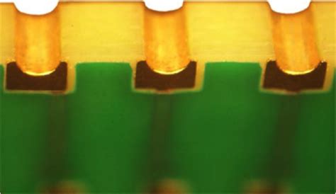
Castellated holes, also known as castellations or half-holes, are a type of mounting feature used in printed circuit board (PCB) design and production. Unlike traditional full plated through holes (PTH), castellated holes are semi-circular cut-outs located along the edges of a PCB.
The main purpose of castellated holes is to facilitate the mounting and electrical connection of a module PCB to a carrier board. The module PCB fits perpendicularly into the castellated holes, with solder applied to create secure mechanical and electrical bonds between the two boards.
Key Characteristics of Castellated Holes
Castellated holes have several distinguishing features:
- Semi-circular cut-out shape
- Located along PCB edges
- Plated with conductive material (e.g., copper)
- Used for module mounting and interconnection
Advantages of Using Castellated Holes
Space Savings
One of the primary advantages of using castellated holes is the space savings they offer compared to other mounting methods. Because the module PCB mounts vertically into the carrier board, the overall footprint is significantly reduced. This is especially beneficial in applications where board real estate is limited, such as in compact electronic devices.
Simplified Assembly
Castellated holes simplify the assembly process by eliminating the need for additional connectors or headers. The module PCB can be directly soldered into the castellated holes on the carrier board, reducing the number of components and assembly steps required.
Improved Signal Integrity
Castellated holes provide a direct electrical connection between the module and carrier boards, minimizing the signal path length. This can lead to improved signal integrity and reduced noise, as there are fewer interconnects and potential points of failure.
Enhanced Mechanical Stability
The perpendicular mounting of the module PCB into the castellated holes creates a strong mechanical bond when soldered. This enhanced mechanical stability is particularly important in applications subject to vibration or shock, ensuring the reliability of the electrical connections.

Design Considerations for Castellated Holes
When incorporating castellated holes into PCB designs, several key factors must be considered to ensure optimal performance and manufacturability.
Hole Size and Spacing
The size and spacing of castellated holes are critical design parameters. The hole diameter should be large enough to accommodate the thickness of the module PCB while allowing for proper solder fillets to form. The spacing between holes must also be sufficient to maintain PCB structural integrity and prevent solder bridging.
Typical castellated hole sizes range from 0.5mm to 1.0mm in diameter, with a minimum spacing of 0.8mm to 1.2mm between holes.
Plating Requirements
Castellated holes require plating to establish reliable electrical connections. The plating process involves applying a conductive layer, typically copper, to the inside surfaces of the holes. This plating must be of sufficient thickness and quality to ensure good solderability and current-carrying capacity.
Common plating specifications for castellated holes include:
| Parameter | Typical Value |
|---|---|
| Copper Plating Thickness | 20-35 µm |
| Minimum Hole Wall Plating | 15 µm |
| Solder Mask Webbing | 50-75 µm |
Solder Mask Design
Proper solder mask design is essential for successful castellated hole assembly. The solder mask helps to prevent solder bridging and short circuits by confining the solder to the desired areas.
For castellated holes, the solder mask should be pulled back slightly from the edge of the hole, creating a web-like structure. This webbing ensures that the solder flows into the hole and forms a reliable connection with the module PCB.
Hole Placement and Edge Clearance
The placement of castellated holes along the PCB edge must consider the required clearances for assembly and manufacturability. Sufficient space should be provided between the holes and the board edge to prevent damage during depaneling and handling.
Minimum edge clearances for castellated holes typically range from 0.25mm to 0.5mm, depending on the PCB thickness and manufacturing capabilities.

PCB Fabrication Process for Castellated Holes
The fabrication of PCBs with castellated holes involves several specialized steps to ensure the proper formation and plating of the holes.
Drilling and Routing
Castellated holes are typically created using a combination of drilling and routing processes. First, small pilot holes are drilled at the locations where the castellations will be formed. These pilot holes serve as reference points for the subsequent routing step.
Next, a high-speed router is used to create the semi-circular cut-outs that form the castellated holes. The router follows the edge of the PCB, removing material to create the desired hole shape and size.
Plating
After the castellated holes are formed, they must be plated to create conductive surfaces for soldering. The plating process involves several steps:
-
Cleaning: The PCB is cleaned to remove any debris or contaminants that may affect plating quality.
-
Electroless Copper: A thin layer of electroless copper is deposited onto the PCB, including the surfaces of the castellated holes. This layer acts as a seed for subsequent electroplating.
-
Electroplating: Additional copper is electroplated onto the PCB, building up the thickness of the conductive layer. This step ensures sufficient current-carrying capacity and solderability.
-
Finish Plating: A final finish, such as immersion gold or ENIG (Electroless Nickel Immersion Gold), may be applied to protect the copper and enhance solderability.
Solder Mask Application
Once plating is complete, a solder mask is applied to the PCB. For castellated holes, the solder mask is typically applied using a liquid photoimageable (LPI) process.
The LPI solder mask is selectively exposed and developed to create openings around the castellated holes while maintaining the required webbing. This webbing helps to control the flow of solder during assembly.
Inspection and Testing
Throughout the fabrication process, various inspections and tests are performed to ensure the quality and reliability of the castellated holes.
Some common inspection and testing methods include:
- Visual inspection
- Automated optical inspection (AOI)
- Electrical continuity testing
- Cross-sectional analysis
These tests help to identify any defects or issues with the castellated holes, such as insufficient plating, solder mask violations, or dimensional inaccuracies.

Assembly Considerations for Castellated Holes
When assembling PCBs with castellated holes, there are several considerations to keep in mind to ensure a successful and reliable outcome.
Solder Paste Application
Solder paste is applied to the castellated holes prior to the placement of the module PCB. The paste can be applied using a stencil printing process or dispensed directly into the holes.
It is important to control the amount of solder paste applied, as excessive paste can lead to bridging or short circuits, while insufficient paste may result in weak or incomplete solder joints.
Module Placement
The module PCB is carefully aligned and inserted into the castellated holes on the carrier board. Proper alignment is critical to ensure that the module makes contact with the plated surfaces of the holes.
Automated placement equipment, such as pick-and-place machines, can be used to achieve accurate and consistent module placement.
Reflow Soldering
After the module PCB is placed, the assembly undergoes a reflow soldering process. During reflow, the solder paste melts and flows, creating a metallurgical bond between the module and carrier boards.
The reflow profile must be carefully controlled to ensure proper solder joint formation without causing damage to the components or PCBs.
Inspection and Rework
After soldering, the assembled PCBs are inspected to verify the quality of the solder joints and the overall integrity of the castellated hole connections.
Automated optical inspection (AOI) and X-ray inspection are commonly used to detect any defects or anomalies.
If issues are found, rework may be necessary to repair or replace the affected components or connections. Specialized rework tools and techniques are employed to minimize the risk of damage to the PCBs during the rework process.
Frequently Asked Questions (FAQ)
- What are the main advantages of using castellated holes in PCB design?
- Space savings due to vertical module mounting
- Simplified assembly without additional connectors
- Improved signal integrity and reduced noise
-
Enhanced mechanical stability through strong solder joints
-
What are the typical sizes and spacings for castellated holes?
- Hole diameters range from 0.5mm to 1.0mm
- Minimum spacing between holes is 0.8mm to 1.2mm
-
Edge clearances of 0.25mm to 0.5mm are recommended
-
What plating requirements are necessary for castellated holes?
- Copper plating thickness of 20-35 µm
- Minimum hole wall plating of 15 µm
-
Solder mask webbing of 50-75 µm
-
How are castellated holes created during PCB fabrication?
- Pilot holes are drilled at castellation locations
- A high-speed router creates the semi-circular cut-outs
- Plating is applied to create conductive surfaces
-
Solder mask is selectively applied with webbing
-
What are the key considerations for assembling PCBs with castellated holes?
- Controlled application of solder paste
- Accurate alignment and placement of the module PCB
- Careful reflow soldering to form reliable joints
- Thorough inspection and rework processes
By understanding the design, fabrication, and assembly considerations for castellated holes, PCB designers and manufacturers can effectively incorporate this versatile mounting method into their products. With proper planning and execution, castellated holes offer significant benefits in terms of space savings, simplified assembly, signal integrity, and mechanical stability.


Leave a Reply