Introduction
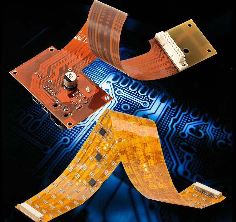
Flex PCBs (flexible printed circuit boards) are a type of PCB that can bend and flex. They allow circuitry to move freely and adapt to different shapes. Flex PCBs are useful for products where flexibility and mechanical articulation are needed. Examples include wearable devices, medical devices, robotics, folded or rolled devices like cameras and laptops.
Altium Designer is a popular PCB design software that provides features to easily design flex PCBs. This article will go over considerations and best practices for designing flex PCBs in Altium, including layout, routing, component placement, and manufacturing design rules.
Benefits of Flex PCBs

Some key benefits of using flex PCBs:
- Flexible – Can bend, fold, twist, and adapt to 3D shapes. Allows movement and articulation.
- Lightweight – Weigh less than rigid PCBs.
- Thin and small – Very thin with small features and spacing.
- Reliability – Flexible construction absorbs shock/vibration.
- Customizable – Can have sections of different stiffness (rigid-flex).
- Complex shapes – Can integrate with non-flat and curved surfaces.
- Packaging – Fits into tight spaces and small products.
Flex PCBs open up many possibilities not attainable with rigid PCBs. Products can be made thinner, lighter, with new form factors. Flex PCBs are especially suited for wearables, medical devices, sensors, antennas, and consumer electronics.
Flex PCB Materials
The base material for flex PCB fabrication is a flexible dielectric film such as polyimide. Common thickness range from 12.5 um to 100 um. The most popular flex PCB material is polyimide (Dupont Kapton).
The conductive layers are typically very thin copper foil, such as 12 um to 35 um thickness. The thin layers allow for flexibility. Minimum trace/space is typically 50/50 um (2/2 mil).
Coverlay, soldermask and stiffeners may be applied to define solder pads, insulate traces, and provide rigidity to sections. Components are attached with conductive or non-conductive epoxy adhesives.
Altium Flex PCB Layout Guidelines
Designing a flex PCB in Altium requires following certain layout practices and constraints to ensure the PCB can actually flex as intended without any failures. Here are some key guidelines:
- Avoid 90 degree angles – Use rounded/tapered corners and teardrop pads. This prevents traces from cracking under bend stress.
- No brittle materials – Don’t use gold or nickel plating. Use rolled annealed copper which is more flexible.
- Minimize components – Place fewer components in the bend area. Adhesives can crack under flexing.
- Wider traces/spacing in flex area – Use at least 6 mil traces with 6+ mil spacing in flexing sections.
- No via stitching – Avoid via stitches in the bend area which can crack.
- Pad size for adhesive – Use larger pad sizes for glue epoxy fillets and bonding.
- Outline cuts and routing – Use rounded/oblong slot cuts instead of sharp corners.
- Stiffeners to control flex – Add stiffeners on flexible sections that should remain rigid.
- Reduce layers – 2 layer flex PCBs are most flexible. Avoid 4-6 layers in bend areas.
Following these guidelines will result in a design that can flex without risk of traces cracking or pads lifting during use. Altium provides constraints and design rules to enforce many of these requirements.
Creating a Flex PCB in Altium
Starting a new flex PCB design in Altium is straightforward. Here is the general process:
- Select File > New > Flexible Board to start a new flex PCB project.
- Set the number of layers, materials, and thickness in the New Flexible Board dialog. Common is 2-layer with polyimide film.
- Create the board shape and cutouts. Use rounded slots and edge corners.
- Set the flex bend areas with a mechanical layer. This defines the bend constraints.
- Assign flex-specific design rules for trace widths, spacing, annular rings.
- Layout components and routing per flex guidelines away from flex zones.
- Add stiffeners, coverlay, soldermask, markings as needed.
- Run design rule checks and simulations to verify the design.
- Output Gerber and fabrication/assembly files.
Altium provides many interactive tools, widgets, and autorouter settings to facilitate flex PCB design as per constraints. The key steps when laying out flex PCBs in Altium are covered next.
Placing Components and Routing
Component placement and routing for flex PCBs requires special care around bend areas. Here are some tips:
- Leave bend areas clear of components. Place components in rigid sections.
- Route traces along the rigid-flex boundary, avoiding flex zones.
- For traces crossing flex zones perpendicular, make them wider and increase spacing.
- Add teardrop pads on traces crossing flex sections.
- Avoid vias, stubs, and parallel traces in flex areas.
- Use larger pad sizes for glue epoxy bonding.
- Verify trace width/spacing rules are met in all sections.
- Bridging rigid sections requires carefully designed flex cables.
Careful planning is needed to place parts and route traces following these practices. Sections that will bend should be left mostly clear of traces and vias. An Autorouter can help route traces efficiently with awareness of rigid/flex areas.
Defining Bending Zones
Altium provides a mechanical layer to designate sections of the PCB that will bend during use. This is defined as:
- Flex Area – Area that will bend repeatedly. Strict constraints on traces.
- Bend Area – Area that bends but less frequently. Moderate constraints.
- Rigid Area – Area that does not bend. Standard PCB rules.
The mechanical layer determines which design rules are enforced in each section. Traces crossing from rigid to flex areas require teardrops, wider spacing, and gradual fanning out. Mechanical layer definitions ensure the PCB can flex without damage.
Managing Layer Stack and Stiffeners
A flex PCB will often have a combination of flexible layers and rigid layers. The layer stackup can be defined in Altium:
- Core layers use a flexible dielectric such as polyimide.
- Outer layers use a thin rolled copper.
- Stiffeners can be incorporated by adding thicker dielectric layers.
- Coverlay adds insulation over traces.
- Mask layers protect and prevent solder leeching.
Stiffeners are sections of thicker rigid fiberglass added to an otherwise flexible PCB. Stiffeners provide rigidity and component mounting. They serve as “islands” on the flex PCB.
The layer stack, materials, and stiffeners can be configured in the Layer Stack Manager when designing a flex PCB in Altium.
Design Rules and Constraints
Altium provides specialized design rules (DRC) for flex PCBs that enforce constraints unique to flexible circuits:
- Trace width/spacing – Minimum widths increased in flex zones.
- Annular rings – Larger annular pads used for adhesive bonding.
- Acute angles – Enforces minimum angle > 90 degrees.
- Teardrops – Mandatory in rigid-to-flex transitions.
- Pad shape – Rounded rectangle pads used.
- Via sizes – Larger microvias with capture pads.
- Stitching vias – Prohibited in bend areas.
The rules prevent features that would compromise reliability and withstand flexing stresses. Rules can be customized per flex/rigid zone requirements. The design rules system automates checking of constraints.
Manufacturing Overview
Once designed, flex PCBs are fabricated using a photolithographic process similar to rigid PCBs. Some key steps:
- Etching copper layers on polyimide dielectric.
- Laser cutting of outlines with rounded corners.
- Coverlay application for insulation.
- Soldermask overlay on pads.
- AOI inspection.
- Stencil printing solder paste.
- Component placement.
- Reflow soldering.
- Adhesive curing.
- Electrical testing.
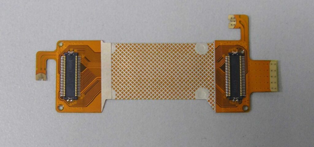
Common connectors on flex PCBs are FFC/FPC – flexible flat cables that terminate in ZIF/LIF connectors. The thin flexible cables can fold easily.
Careful consideration of manufacturability and assembly is important when designing flex PCBs. Factors like material selection, adhesives, and connectors affect reliability.
Applications of Flex PCBs
Some common applications that benefit from using flex PCBs:
- Wearable devices – Fitness bands, smart watches, health trackers.
- Medical – Implants, probes, sensors that flex and bend.
- Consumer electronics – Cell phones, display screens, cameras.
- Robotics – Arms, joints, grippers that require articulation.
- IoT devices – Flexible sensors, antennas, interconnects.
- Auto – Sensors and circuits subject to vibration.
- Aerospace – Circuits that must withstand G-forces and flexing.
As electronics become smaller, more lightweight, and structurally dynamic, flex PCBs provide the electrical connections that can withstand the demands.
Pros and Cons of Flex PCBs
Some key advantages and disadvantages when using flex PCBs:
Pros
- Highly flexible and dynamic.
- Thin, lightweight. Saves space.
- Bendable sections and 3D forms.
- Vibration/shock resistance.
- Integrates rigid and flex regions.
- Complex shapes fit design needs.
Cons
- Limited component mounting in flex areas.
- Requires special layout considerations.
- Fabrication process more complex than rigid PCBs.
- Requires adhesives for assembly.
- Can experience conductor cracks over time.
- Relatively higher cost than rigid PCBs.
Understanding the tradeoffs allows selecting flex PCBs when the benefits are needed for a particular product. As flex PCB technology and design tools improve, the advantages continue to grow over rigid PCBs.
Frequently Asked Questions
Q: What are some typical board thickness values for flex PCBs?
A: Flex PCB thickness typically ranges from about 50 um to 150 um. Very thin flex PCBs can be 25 um. Common values are 50 um (2 mil), 75 um, and 100 um (4 mil). The thin profile is a key benefit of flex circuits.
Q: Do flex PCBs require special soldering methods?
A: Yes, reflow soldering of flex PCB requires precise temperature control. The thin flexible material expands and contracts at different rates compared to FR4. The reflow process needs to accommodate this to avoid damage.
Q: Can flex PCBs have components on both sides?
A: Yes, but components are usually just on one side in the rigid areas. Having components on both sides increases stiffness. It also makes assembly more difficult. One-sided placement allows the flex area to remain thin.
Q: What are some methods for connecting flex PCBs to rigid PCBs?
A: Common approaches are soldered tabs, edge fingers, FFC/FPC connectors, and Zebra strips. Careful design is needed to provide both mechanical strength and electrical connection.
Q: How many bend cycles can flex PCBs withstand?
A: Testing has shown flex PCBs can exceed 25,000 bend cycles before failures may occur. This depends on trace widths, materials, bend radius, and other factors. Careful design provides very long flex life.
Conclusion
Flex PCBs provide many advantages in products requiring thin, lightweight, and dynamic circuitry. Altium Designer provides a robust set of tools to efficiently design flex PCBs adhering to specialized constraints and layout rules. With sound layout practices, simulations, and design rule verification, flex PCBs can be designed that reliably withstand mechanical articulation and repeated bending. The applications leveraging flex PCB technology will undoubtedly continue expanding as products become more compact, portable, and wearable.


Leave a Reply