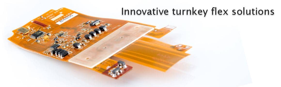
Introduction to Flex PCBs
A flexible printed circuit board (flex PCB or flex circuit) is a type of printed circuit board that is made of flexible materials such as polyimide. Unlike traditional rigid PCBs, flex PCBs can bend and flex. This allows them to be used in applications where a rigid board would not be suitable.
Flex PCBs have conductors and other components printed/etched onto a flexible dielectric substrate. They are often used to interconnect rigid PCBs and can fold into three-dimensional configurations. They are lightweight, durable, and well suited for dynamic flexing applications.
Advantages of Flex PCBs
- Can conform to uneven surfaces and move dynamically
- Thin, lightweight, and flexible
- Durability and flex life
- Space and weight savings
- Design freedom and integration
- Lower assembly costs
They are commonly used in the following industries/applications:
- Consumer electronics
- Medical devices
- Industrial automation
- Military and aerospace
- Automotive
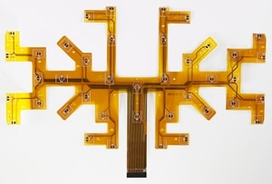
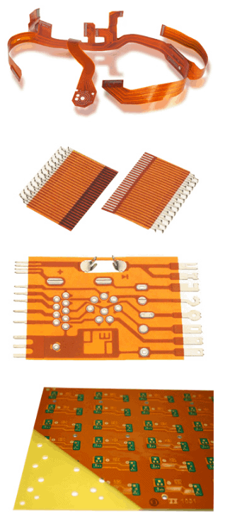
Types of Flex PCBs
There are three main types of flex PCB configurations:
Single Sided Flex Circuits: Conductors on only one side of the substrate.
Double Sided Flex Circuits: Conductors on both sides of the substrate. Allows for higher circuit density.
Multilayer Flex Circuits: Flex boards with 3 or more conductive layers allowing for even greater density.
Benefits of 2 Layer Flex PCBs
2 layer flex PCBs are the most common and cost-effective type of flexible printed circuit boards. They offer several benefits over single sided flex circuits:
- Higher circuit density: 2 conductive layers allow you to design more compact and complex circuits vs single layer.
- Lower costs: They are cheaper to produce than 4+ layer flex circuits.
- Easier manufacturing: 2 layer flex PCBs are easier to manufacturer compared to multilayer flex.
- Flexibility: They provide good flexibility while maintaining circuit density.
- Signal isolation: Top and bottom layers can be used for power and ground planes to isolate signals.
For many applications, 2 layer flex provides the ideal balance of density, cost, manufacturability, and performance. They are a versatile flex PCB option suitable for a wide range of products.
Design Considerations for 2 Layer Flex PCBs
There are several important design considerations when working with 2 layer flexible PCBs:
Layer Stackup
A typical 2 layer flex PCB stackup consists of:
- Coverlayer: A thin flexible dielectric layer on the top and bottom. Usually polyimide. Protects conductors.
- Conductors: Copper traces etched on top and bottom layers.
- Dielectric Core: Flexible insulating substrate (polyimide) between layers.
- Adhesive: Bonds layers together. Can be acrylic or epoxy based.
Conductor Thickness
1/2 oz (17 um) or 1 oz (35 um) copper thickness is commonly used. 1/2 oz is more flexible while 1 oz offers better durability and current carrying capacity.
Conductor/Space/Gap
The width and spacing of conductors is an important consideration. Narrower traces allow higher density but limit current capacity. Typical design rules are:
- Minimum trace width: 4-10 mils (0.1-0.25mm)
- Minimum spacing: 4-6 mils (0.1-0.15mm)
Bend Radius
Flex PCBs should not be folded sharper than their minimum bend radius or it will damage the conductors. Typical bend radius range is 2-10x the board thickness.
Stiffeners
Strategically placed stiffeners (rigid sections) can be added to control flexibility and access components. Stiffeners are typically polyimide or aluminum.
Vias
Used to connect layers and components. Typical via diameters are 0.2-0.5mm. Laser drilled or mechanically punched.
Terminations
Pads/lands for component termination should be tented (covered with soldermask) to prevent wicking.
manufacturability
To ensure reliable manufacturing, work closely with your flex PCB manufacturer during the design process. Here are some key manufacturability guidelines:
Panel Utilization
Flex PCBs are typically produced in panel form for efficiency then singulated. Optimize individual PCB size/layout to maximize panel utilization.
Grain Direction
All conductors should be oriented along the same axis as the grain direction of the flex material for optimal performance.
Symmetric Layer Stacking
Keep layer 1 and 2 features symmetrically aligned to avoid distortion or tenting during lamination.
Controlled Impedance
If controlled impedance traces are required, coordinate impedance requirements and stackup with your PCB manufacturer early in the design flow.
Tolerances
Account for typical flex PCB manufacturing tolerances in your design:
- Conductor width/space: +/- 4%
- Hole diameter: +/- 8%
- Registration: +/- 0.10mm
- Bow and twist: +/- 2.5mm per 100mm
Assembly Considerations
Here are some considerations for assembly of components onto 2 layer flex PCBs:
Component Types: Use surface mount components as much as possible. Avoid large/heavy through-hole parts which can put excessive stress on vias.
Adhesives: Use flexible adhesives like silicones or acrylics to attach components. Avoid rigid adhesives.
Strain relief: Provide adequate support/strain relief for connectors and heavy components to reduce stresses.
Flex folds: Folds/bends should be in one direction and at least 10x material thickness from any component.
ESD protection: Flex boards are prone to ESD damage. Use proper ESD handling procedures.
Soldering: Use soldering irons under 700°F. Avoid soldering stress on boards.
Inspection: Inspect for lifted pads, cracked joints, pinholes/voids after assembly.
Applications of 2 Layer Flex PCBs
Here are some common applications where 2 layer flex PCBs provide excellent solutions:
Wearable electronics
- Fitness trackers
- Smart watches
- Health monitoring devices
Consumer electronics
- Laptops
- Digital cameras
- Mobile phones
- LED lighting
Medical
- Hearing aids
- Blood pressure monitors
- Ultrasound probes
Automotive
- Seat heaters
- Overhead consoles
- Sensors
Industrial
- Robotics
- Automation systems
- IoT devices
With their design flexibility, durability, and cost advantages, 2 layer flex PCBs are an enabling technology across a wide range of markets and applications.
FQA about 2 Layer Flex PCBs
Here are answers to some frequently asked questions about 2 layer flex PCBs:
What are the typical dielectric materials used in 2 layer flex PCBs?
The most common dielectric core material is polyimide (PI). Other options include PET, PEN, PEI. Polyimide provides the best thermal stability and chemical resistance.
What are the thickness options for 2 layer flex boards?
Typical thickness range is from 25um to 150um. Thinner flex materials provide maximum flexibility while thicker material offers better ruggedness and component mounting.
Can 2 layer flex PCBs incorporate rigid sections?
Yes, rigid segments (stiffeners) can be incorporated by using thicker dielectric materials, attached rigid substrates, or stiffening coatings/inks. This allows integration of ICs or connectors.
What are typical minimum bend radii for 2 layer flex PCBs?
The minimum bend radius is usually expressed as a multiple of the total board thickness. A typical range is 2-10X the thickness. For a 100um flex PCB, the minimum bend radius would be 200um-1000um (0.2mm-1mm).
What types of connectors can be used with 2 layer flex circuits?
Common connector options include: anisotropic conductive film (ACF), zero insertion force (ZIF), pressure contacts, crimped terminals, soldered joints, adhesive bonding. The best choice depends on the application.


Leave a Reply