What is a PWB?
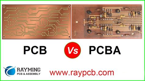
A printed wiring board (PWB), also known as a printed circuit board (PCB), is the foundation of most modern electronic devices. It is a flat board made of insulating material, such as fiberglass or composite epoxy, with conductive copper tracks printed or etched onto the surface. These copper tracks connect various electronic components, such as resistors, capacitors, and integrated circuits, to create a complete electronic circuit.
PWBs have revolutionized the electronics industry by providing a reliable, compact, and cost-effective means of assembling electronic circuits. They have enabled the development of increasingly complex electronic devices while reducing their size and weight.
PWB Materials
Substrate Materials
The choice of substrate material is crucial in determining the performance and reliability of a PWB. The most common substrate materials used in PWB manufacturing are:
-
FR-4: A composite material made of woven fiberglass cloth with an epoxy resin binder. It is the most widely used substrate material due to its excellent mechanical and electrical properties, as well as its cost-effectiveness.
-
High Tg FR-4: A variant of FR-4 with a higher glass transition temperature (Tg), which improves its thermal stability and resistance to warping.
-
Polyimide: A high-performance polymer with excellent thermal and chemical resistance, making it suitable for applications in harsh environments.
-
PTFE: Polytetrafluoroethylene, also known as Teflon, is a low-dielectric constant material with excellent high-frequency performance and thermal stability.
| Material | Dielectric Constant | Thermal Conductivity (W/mK) | Tg (°C) |
|---|---|---|---|
| FR-4 | 4.5 | 0.3 | 130-140 |
| High Tg FR-4 | 4.5 | 0.3 | 170-180 |
| Polyimide | 3.5 | 0.2 | 250-400 |
| PTFE | 2.1 | 0.2 | 327 |
Copper Foil
Copper foil is the conductive material used to create the Circuit Traces on a PWB. It is available in various thicknesses, typically ranging from 0.5 oz/ft² (18 µm) to 2 oz/ft² (70 µm). The choice of copper thickness depends on the current-carrying requirements of the circuit and the manufacturing process.

PWB Manufacturing Process
The PWB manufacturing process involves several steps, each of which contributes to the quality and reliability of the final product.
1. Design and Layout
The first step in PWB manufacturing is the design and layout of the electronic circuit. This involves creating a schematic diagram of the circuit and then translating it into a physical layout using specialized software. The layout determines the position and routing of the copper traces, as well as the placement of components on the board.
2. Film Generation
Once the layout is complete, the next step is to generate the artwork films used to transfer the circuit pattern onto the copper-clad substrate. This is typically done using a high-resolution printer or plotter.
3. Etching
The copper-clad substrate is then coated with a light-sensitive photoresist and exposed to UV light through the artwork films. This hardens the photoresist in the areas that will become the copper traces. The unexposed photoresist is then removed, leaving the desired circuit pattern.
The board is then immersed in an etching solution, typically ferric chloride or ammonium persulfate, which removes the unwanted copper, leaving only the circuit traces protected by the hardened photoresist.
4. Drilling
After etching, the board undergoes a drilling process to create holes for through-hole components and vias. Vias are small holes that connect different layers of a multi-layer PWB.
5. Plating
The drilled holes are then plated with copper to create electrical connections between layers. This is followed by a tin-lead or lead-free solder plating process to protect the copper and provide a solderable surface for component attachment.
6. Solder Mask and Silkscreen
A solder mask, typically green in color, is applied to the board to protect the copper traces from oxidation and prevent solder bridging during component assembly. A silkscreen layer is then added to provide component labels and other markings.
7. Surface Finish
Finally, a surface finish is applied to the exposed copper areas to protect them from oxidation and enhance solderability. Common surface finishes include:
- Hot Air Solder Leveling (HASL)
- Electroless Nickel Immersion Gold (ENIG)
- Immersion Silver
- Immersion Tin
- Organic Solderability Preservative (OSP)

PWB Types
PWBs can be classified based on the number of layers and the type of components they accommodate.
Single-Layer PWBs
Single-layer PWBs have copper traces on only one side of the substrate. They are the simplest and most cost-effective type of PWB but are limited in terms of circuit complexity and component density.
Double-Layer PWBs
Double-layer PWBs have copper traces on both sides of the substrate, allowing for more complex circuits and higher component density compared to single-layer boards.
Multi-Layer PWBs
Multi-layer PWBs consist of three or more layers of copper traces separated by insulating layers. They offer the highest level of circuit complexity and component density but are also the most expensive to manufacture.
| PWB Type | Layers | Complexity | Cost |
|---|---|---|---|
| Single-Layer | 1 | Low | Low |
| Double-Layer | 2 | Medium | Medium |
| Multi-Layer | 3+ | High | High |
Through-Hole PWBs
Through-hole PWBs are designed to accommodate components with leads that are inserted through holes drilled in the board and soldered to pads on the opposite side. They are well-suited for applications that require high mechanical strength and reliability.
Surface Mount PWBs
Surface mount PWBs are designed for components that are soldered directly onto pads on the surface of the board. Surface mount technology (SMT) allows for smaller components and higher component density compared to through-hole technology.
Mixed Technology PWBs
Mixed technology PWBs combine through-hole and surface mount components on the same board, offering the benefits of both technologies.

PWB Design Considerations
When designing a PWB, several factors must be taken into account to ensure optimal performance, reliability, and manufacturability.
1. Signal Integrity
Signal integrity refers to the ability of a PWB to transmit signals without degradation. Factors that can affect signal integrity include:
- Trace width and spacing
- Trace impedance
- Crosstalk
- Reflections
- Electromagnetic interference (EMI)
Proper design techniques, such as impedance matching, differential signaling, and proper grounding, can help maintain signal integrity.
2. Power Integrity
Power integrity refers to the ability of a PWB to deliver clean, stable power to all components. Factors that can affect power integrity include:
- Voltage drop
- Power supply noise
- Ground bounce
- Decoupling capacitor placement
Proper power plane design, decoupling, and power supply filtering can help maintain power integrity.
3. Thermal Management
Thermal management is critical in ensuring the long-term reliability of a PWB and its components. Factors that can affect thermal performance include:
- Power dissipation of components
- Copper thickness and distribution
- Airflow and cooling solutions
Proper component placement, copper balance, and the use of thermal vias and heatsinks can help manage heat dissipation.
4. Manufacturing Constraints
PWB design must also consider the limitations and capabilities of the manufacturing process. Factors to consider include:
- Minimum trace width and spacing
- Minimum hole size
- Aspect ratio of holes
- Copper thickness and uniformity
- Solder mask and silkscreen registration
Adherence to industry standards, such as IPC, can help ensure manufacturability and reliability.
FAQ
1. What is the difference between a PWB and a PCB?
A printed wiring board (PWB) and a printed circuit board (PCB) are essentially the same things. Both terms refer to a flat board with conductive tracks used to connect electronic components. However, some people use “PWB” to refer specifically to boards with wires or cables attached, while “PCB” is used more broadly.
2. What is the most common substrate material used in PWBs?
FR-4, a composite material made of woven fiberglass cloth with an epoxy resin binder, is the most widely used substrate material in PWBs due to its excellent mechanical and electrical properties, as well as its cost-effectiveness.
3. What is the purpose of solder mask on a PWB?
The solder mask is a protective coating applied to the copper traces on a PWB. It serves to:
- Protect the copper from oxidation
- Prevent solder bridging during component assembly
- Provide electrical insulation between adjacent traces
- Improve the aesthetics of the board
4. What is the difference between through-hole and surface mount components?
Through-hole components have leads that are inserted through holes drilled in the PWB and soldered to pads on the opposite side. They offer high mechanical strength and reliability but require more space and are more labor-intensive to assemble.
Surface mount components are soldered directly onto pads on the surface of the PWB. They are smaller, allow for higher component density, and are better suited for automated assembly processes. However, they may be more susceptible to thermal and mechanical stress.
5. Why is signal integrity important in PWB design?
Signal integrity is crucial in ensuring that electronic signals are transmitted accurately and reliably through a PWB. Poor signal integrity can lead to issues such as:
- Signal distortion and attenuation
- Crosstalk between adjacent traces
- Electromagnetic interference (EMI)
- Timing errors and data corruption
By adopting proper design techniques, such as impedance matching, differential signaling, and proper grounding, designers can maintain signal integrity and ensure the optimal performance of the electronic circuit.


Leave a Reply