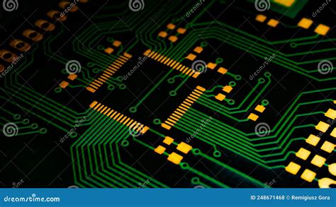
What is Circuit Trace?
Circuit trace, also known as PCB trace or simply trace, refers to the copper paths that electrically connect different components on a printed circuit board (PCB). These traces act as the wires in a circuit, allowing signals and power to flow between various parts of the board. Circuit traces are an essential aspect of PCB design, as they determine the functionality, reliability, and performance of the final product.
Key Characteristics of Circuit Traces
| Characteristic | Description |
|---|---|
| Width | The width of the trace determines its current-carrying capacity and impedance. |
| Thickness | Trace thickness affects the current-carrying capacity and the manufacturing process. |
| Length | Trace length influences signal integrity, especially at high frequencies. |
| Shape | Traces can be straight, curved, or angled, depending on the design requirements. |
| Material | Copper is the most common material used for circuit traces due to its excellent electrical conductivity. |
Designing Circuit Traces
Trace Width and Thickness
The width and thickness of a circuit trace are crucial factors in PCB design. The trace width determines the amount of current the trace can carry without overheating or causing voltage drops. The thickness, on the other hand, affects the trace’s resistance and current-carrying capacity.
To calculate the appropriate trace width, designers use the following factors:
– Current requirements
– Ambient temperature
– Trace thickness
– Copper weight
– Maximum allowable temperature rise
There are various online calculators and tools available to help designers determine the optimal trace width based on these factors.
Trace Spacing and Clearance
In addition to trace width and thickness, designers must also consider the spacing between traces and the clearance between traces and other components. Proper spacing and clearance are essential to prevent short circuits, signal interference, and manufacturing issues.
The minimum trace spacing and clearance depend on several factors, such as:
– PCB manufacturing capabilities
– Voltage levels
– Operating environment
– Applicable standards and regulations
Designers often refer to the PCB manufacturer’s design guidelines and industry standards, such as IPC-2221, to determine the appropriate spacing and clearance for their designs.
Signal Integrity Considerations
Signal integrity is a critical aspect of circuit trace design, particularly for high-speed and high-frequency applications. Poor signal integrity can lead to issues such as crosstalk, reflections, and electromagnetic interference (EMI).
To maintain signal integrity, designers employ various techniques, such as:
– Impedance matching
– Termination
– Differential pair routing
– Ground planes and power planes
– Shielding and grounding
By carefully designing circuit traces and implementing these techniques, designers can ensure the proper functioning and reliability of the PCB.

Manufacturing Circuit Traces
PCB Fabrication Process
The manufacturing of circuit traces is an integral part of the PCB fabrication process. The most common method for creating circuit traces is through a combination of photolithography and etching.
The basic steps in the PCB fabrication process are:
1. Substrate preparation
2. Copper cladding
3. Photoresist application
4. Exposure and development
5. Etching
6. Photoresist removal
7. Inspection and testing
Copper Weight and Thickness
The amount of copper used in the PCB is referred to as the copper weight, which is typically measured in ounces per square foot (oz/ft²). Common copper weights include 0.5 oz/ft², 1 oz/ft², and 2 oz/ft².
The thickness of the copper layer is directly related to the copper weight. For example, a 1 oz/ft² copper weight translates to a thickness of approximately 35 microns (1.4 mils).
| Copper Weight (oz/ft²) | Thickness (microns) | Thickness (mils) |
|---|---|---|
| 0.5 | 17.5 | 0.7 |
| 1 | 35 | 1.4 |
| 2 | 70 | 2.8 |
Choosing the appropriate copper weight and thickness depends on the specific requirements of the PCB, such as current-carrying capacity, thermal management, and mechanical strength.
Surface Finishes
After the etching process, the exposed copper traces are susceptible to oxidation and corrosion. To protect the traces and enhance solderability, various surface finishes can be applied to the PCB.
Common surface finishes include:
– Hot Air Solder Leveling (HASL)
– Organic Solderability Preservative (OSP)
– Electroless Nickel Immersion Gold (ENIG)
– Immersion Silver
– Immersion Tin
Each surface finish has its advantages and disadvantages in terms of cost, durability, and compatibility with different assembly processes.

Testing and Inspection
Electrical Testing
Electrical testing is performed to ensure that the manufactured PCB meets the designed specifications and functions as intended. There are several types of electrical tests, including:
- Continuity test: Verifies that the proper connections exist between the various components and tracks on the PCB.
- Isolation test: Checks for any unwanted short circuits between tracks or components that should be electrically isolated.
- Resistance test: Measures the resistance of the traces to ensure they meet the specified values.
- High-potential (HiPot) test: Applies a high voltage to the PCB to detect any insulation breakdowns or leakage currents.
Automated Optical Inspection (AOI)
Automated Optical Inspection (AOI) is a computer-based system that uses cameras and image processing software to inspect PCBs for defects. AOI systems can detect various issues, such as:
- Incorrect component placement
- Missing or misaligned components
- Solder bridging or insufficient solder
- Trace defects, such as opens or shorts
AOI is a fast and efficient method for identifying defects early in the manufacturing process, reducing the risk of costly rework or failures in the final product.
X-ray Inspection
X-ray inspection is a non-destructive testing method that allows for the examination of solder joints and other internal features of the PCB. This technique is particularly useful for inspecting components with hidden connections, such as ball grid arrays (BGAs) or flip-chips.
X-ray inspection systems use high-resolution X-ray images to detect defects such as:
– Voids in solder joints
– Insufficient or excessive solder
– Misaligned or bridged connections
– Cracks or fractures in components
By employing X-ray inspection, manufacturers can ensure the quality and reliability of complex PCB assemblies.

Troubleshooting and Repair
Common Circuit Trace Issues
Despite careful design and manufacturing processes, circuit trace issues can still occur. Some common problems include:
- Open traces: A break in the trace that prevents electrical continuity.
- Short circuits: Unintended electrical connections between traces or components.
- Overheated traces: Traces that have been subjected to excessive current, leading to damage or failure.
- Damaged traces: Traces that have been physically damaged due to handling, impact, or environmental factors.
Identifying and resolving these issues promptly is crucial to avoid further damage and ensure the proper functioning of the PCB.
Troubleshooting Techniques
When faced with circuit trace issues, designers and technicians can employ various troubleshooting techniques to identify and resolve the problem. Some common approaches include:
- Visual inspection: Carefully examining the PCB for any visible signs of damage, such as cracks, burns, or discoloration.
- Continuity testing: Using a multimeter to check for electrical continuity between points on the PCB.
- Thermal imaging: Employing a thermal camera to identify areas of excessive heat, which may indicate overloaded or damaged traces.
- Microscopic inspection: Using a microscope to closely examine traces and components for defects or damage.
- Functional testing: Performing tests to verify the proper operation of the PCB and isolate any malfunctioning areas.
By systematically applying these techniques, troubleshooters can pinpoint the root cause of the issue and develop an appropriate solution.
Repair Methods
Once the cause of the circuit trace issue has been identified, there are several repair methods that can be employed, depending on the nature and extent of the damage.
Some common repair techniques include:
– Jumper wires: Adding a small wire to bridge a damaged or open trace.
– Conductive epoxy: Applying a conductive adhesive to repair broken traces or reconnect components.
– Trace repair kits: Using specialized kits that contain conductive materials and tools for repairing damaged traces.
– Solder bridges: Creating a solder connection to bypass a damaged trace or component.
– PCB rework: Removing and replacing damaged components or sections of the PCB.
The choice of repair method depends on factors such as the accessibility of the damaged area, the severity of the damage, and the available tools and materials.
FAQ
1. What is the difference between a circuit trace and a wire?
While circuit traces and wires both serve the purpose of carrying electrical signals, there are some key differences between the two:
- Circuit traces are flat, copper pathways printed directly onto the PCB substrate, while wires are typically insulated, round conductors.
- Traces are an integral part of the PCB and cannot be easily modified once manufactured, whereas wires are separate components that can be added, removed, or replaced as needed.
- Traces have a fixed width and thickness determined by the PCB design, while wires come in various gauges and insulation materials.
2. Can circuit traces be repaired if damaged?
Yes, circuit traces can often be repaired if damaged, depending on the extent and location of the damage. Common repair methods include:
- Jumper wires
- Conductive epoxy
- Trace repair kits
- Solder bridges
- PCB rework
The choice of repair method depends on factors such as accessibility, severity of the damage, and available tools and materials.
3. What factors influence the current-carrying capacity of a circuit trace?
The current-carrying capacity of a circuit trace depends on several factors, including:
- Trace width: Wider traces can carry more current than narrower traces.
- Trace thickness: Thicker traces have a higher current-carrying capacity than thinner traces.
- Ambient temperature: Higher ambient temperatures reduce the current-carrying capacity of traces.
- Copper weight: Higher copper weights increase the current-carrying capacity of traces.
- Maximum allowable temperature rise: The current-carrying capacity is limited by the maximum allowable temperature rise of the trace.
Designers must consider these factors when calculating the appropriate trace width for a given application.
4. What is the purpose of surface finishes on circuit traces?
Surface finishes are applied to circuit traces for several reasons:
- Protection: Surface finishes protect the exposed copper traces from oxidation and corrosion.
- Solderability: Finishes such as HASL, OSP, and ENIG enhance the solderability of the traces, making it easier to attach components during the assembly process.
- Durability: Some surface finishes, like ENIG, offer increased durability and wear resistance compared to bare copper.
- Compatibility: Different surface finishes are compatible with specific assembly processes and environmental conditions.
The choice of surface finish depends on the specific requirements of the PCB, such as the intended application, assembly process, and environmental factors.
5. How can signal integrity issues be mitigated in circuit trace design?
Signal integrity issues can be mitigated through careful design and implementation of various techniques, such as:
- Impedance matching: Ensuring that the trace impedance matches the source and load impedances to minimize reflections and signal distortion.
- Termination: Adding resistors or other components at the end of traces to absorb reflections and maintain signal quality.
- Differential pair routing: Using two traces with equal and opposite signals to cancel out electromagnetic interference and reduce crosstalk.
- Ground planes and power planes: Incorporating dedicated layers for ground and power distribution to provide a low-impedance return path and reduce noise.
- Shielding and grounding: Using shielding techniques and proper grounding to minimize electromagnetic interference and crosstalk between traces.
By employing these techniques and adhering to best practices in PCB design, signal integrity issues can be effectively mitigated, ensuring the proper functioning and reliability of the circuit.


Leave a Reply