Understanding the Basics of PCB Design
Before diving into specific guidelines, it’s important to understand the basics of PCB design. A printed circuit board is a flat board made of insulating material with conductive tracks on one or both sides. Components are mounted on the board and connected by the tracks to form a complete circuit.
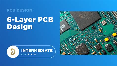
PCBs can be classified based on the number of layers:
| PCB Type | Number of Layers |
|---|---|
| Single-sided | 1 |
| Double-sided | 2 |
| Multi-layer | 4, 6, 8, or more |
The choice of PCB type depends on the complexity of the circuit, the required performance, and the available budget.
Choosing the Right PCB Material
The choice of PCB material is critical for ensuring the board’s performance and reliability. The most common PCB materials are:
- FR-4: A widely used, cost-effective material with good mechanical and electrical properties.
- High Tg FR-4: An improved version of FR-4 with better thermal stability and lower thermal expansion.
- Rogers: A high-performance material with excellent high-frequency and low-loss characteristics.
Consider the following factors when selecting the PCB material:
- Operating temperature range
- Dielectric constant and loss tangent
- Mechanical strength and flexibility
- Cost and availability

Designing for Manufacturing (DFM)
Designing for manufacturing (DFM) is a crucial aspect of PCB design. By following DFM guidelines, you can minimize manufacturing issues, reduce costs, and improve yield. Some key DFM considerations include:
Minimum Track Width and Spacing
Ensure that your design adheres to the manufacturer’s minimum track width and spacing requirements. Typical values are:
| PCB Type | Minimum Track Width | Minimum Spacing |
|---|---|---|
| Standard | 0.2 mm (8 mil) | 0.2 mm (8 mil) |
| High-density | 0.1 mm (4 mil) | 0.1 mm (4 mil) |
Pad Size and Drill Diameter
Use appropriate pad sizes and drill diameters for through-hole components. Typical values are:
| Component Type | Pad Size | Drill Diameter |
|---|---|---|
| Resistors, capacitors | 1.8 mm (70 mil) | 0.8 mm (31 mil) |
| ICs, connectors | 2.5 mm (98 mil) | 1.0 mm (39 mil) |
Solder Mask and Silkscreen
- Ensure adequate solder mask expansion (typically 0.05 mm or 2 mil) around pads to prevent solder bridging.
- Provide clear and legible silkscreen markings for component placement and orientation.

Signal Integrity and EMC Considerations
Signal integrity and electromagnetic compatibility (EMC) are critical aspects of PCB design, especially for high-speed and sensitive circuits. Follow these guidelines to minimize signal integrity issues and EMC problems:
Impedance Control
- Use controlled impedance traces for high-speed signals to minimize reflections and signal distortion.
- Common impedance values are 50Ω for single-ended traces and 100Ω for differential pairs.
Grounding and Power Distribution
- Use a solid ground plane to provide a low-impedance return path for signals and minimize ground bounce.
- Decouple power supplies with appropriate capacitors close to the power pins of ICs.
- Use split power planes or power islands for noise-sensitive circuits.
EMI Reduction Techniques
- Minimize loop areas in high-frequency circuits to reduce electromagnetic radiation.
- Use shielding techniques, such as grounded guard traces or metallic enclosures, to contain EMI.
- Follow proper PCB layout practices, such as avoiding long parallel traces and minimizing cross-talk.

Thermal Management
Proper thermal management is essential for ensuring the reliability and longevity of PCBs, particularly those with high-power components. Consider the following guidelines:
- Use a sufficient copper pour for power and ground planes to improve heat dissipation.
- Provide adequate spacing between high-power components to avoid thermal interaction.
- Use thermal vias to conduct heat from components to the opposite side of the board or to an external heatsink.
- Consider using thermal interface materials, such as Thermal Pads or Thermal Adhesives, to enhance heat transfer.
Documentation and Version Control
Proper documentation and version control are crucial for maintaining the integrity of your PCB design and facilitating future modifications or troubleshooting. Follow these best practices:
- Use a consistent and descriptive naming convention for files and folders.
- Maintain a clear and organized directory structure for your design files.
- Use version control software, such as Git or SVN, to track changes and collaborate with team members.
- Provide comprehensive documentation, including schematics, BOMs, assembly drawings, and test procedures.
Frequently Asked Questions (FAQ)
1. What is the importance of a good PCB design?
A good PCB design ensures the reliability, performance, and cost-effectiveness of the final product. It minimizes manufacturing issues, reduces signal integrity problems, and improves the overall quality of the circuit.
2. How do I choose the right PCB manufacturer?
When choosing a PCB manufacturer, consider factors such as their experience, capabilities, quality control processes, turnaround time, and cost. Look for manufacturers with good references and a proven track record in your industry.
3. What are the most common PCB Design Mistakes to avoid?
Some common PCB design mistakes include violating design rules, neglecting signal integrity, improper grounding and power distribution, ignoring thermal management, and lack of documentation and version control.
4. How can I optimize my PCB design for cost reduction?
To optimize your PCB design for cost reduction, consider using standard materials and components, minimizing the number of layers, using larger track widths and spacings, and avoiding unnecessary features or complexity.
5. What are the key considerations for high-speed PCB design?
Key considerations for high-speed PCB design include impedance control, proper grounding and power distribution, minimizing signal reflections and crosstalk, and following good layout practices to reduce EMI and signal integrity issues.
Conclusion
Designing a high-quality, reliable, and cost-effective PCB requires a deep understanding of the various design guidelines and best practices. By following the guidelines outlined in this article, you can create PCB designs that are optimized for manufacturing, signal integrity, thermal management, and overall performance.
Remember to choose the right materials, follow DFM guidelines, consider signal integrity and EMC, ensure proper thermal management, and maintain comprehensive documentation and version control.
As a PCB engineer, I strongly encourage all designers to continuously learn and stay updated with the latest industry standards and best practices. By doing so, you can create PCB designs that meet the ever-increasing demands of modern electronics and contribute to the success of your projects.


Leave a Reply