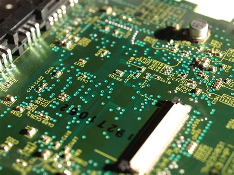
Understanding Printed Circuit Boards
A printed circuit board is a thin board made of insulating materials, such as fiberglass or composite epoxy, with conductive pathways etched or printed onto its surface. These pathways, known as traces, connect the electronic components mounted on the board, allowing electrical signals to flow between them. PCBs provide a stable and compact platform for electronic circuits, making them essential in virtually all modern electronic devices.
Types of PCBs
PCBs can be classified into different types based on their structure and the number of layers:
-
Single-Sided PCBs: These boards have conductive traces on only one side of the insulating substrate. They are the simplest and most cost-effective type of PCB.
-
Double-sided PCBs: These boards have conductive traces on both sides of the insulating substrate. They offer more design flexibility and higher component density compared to single-sided PCBs.
-
Multi-layer PCBs: These boards consist of multiple layers of insulating material and conductive traces stacked on top of each other. They are used in complex electronic devices that require high component density and advanced signal routing.
| PCB Type | Layers | Cost | Design Flexibility |
|---|---|---|---|
| Single-sided PCB | 1 | Low | Limited |
| Double-sided PCB | 2 | Moderate | Increased |
| Multi-layer PCB | 3+ | High | High |
The PCB Assembly Process at RAYPCB
RAYPCB follows a well-defined industrial process for PCB assembly to ensure consistent quality and reliability. The process involves several stages, including:
1. Design and Engineering
The PCB assembly process begins with the design and engineering phase. RAYPCB’s team of experienced engineers works closely with clients to understand their requirements and develop an optimal PCB design. This stage involves:
- Schematic capture: Creating a graphical representation of the electronic circuit using specialized software.
- PCB layout: Arranging the components and routing the traces on the PCB using computer-aided design (CAD) tools.
- Design validation: Checking the design for potential issues, such as signal integrity, electromagnetic compatibility, and manufacturability.
2. PCB Fabrication
Once the PCB design is finalized, it moves to the fabrication stage. RAYPCB partners with reputable PCB manufacturers to ensure the highest quality boards are produced. The fabrication process typically involves:
- Printing the circuit pattern onto the copper-clad laminate using photoresist and etching techniques.
- Drilling holes for through-hole components and vias.
- Applying a solder mask to protect the copper traces and prevent short circuits.
- Adding a silkscreen layer for component labels and other markings.
3. Component Placement
With the fabricated PCB ready, the next step is to place the electronic components onto the board. RAYPCB utilizes advanced surface mount technology (SMT) and through-hole technology (THT) for component placement.
SMT Component Placement
SMT components are placed onto the PCB using automated pick-and-place machines. These machines use vacuum nozzles to pick up the components from reels or trays and place them accurately on the designated pads on the PCB. The process is guided by computer vision systems that ensure precise placement.
THT Component Placement
THT components, such as connectors and large capacitors, are inserted manually or using semi-automatic machines. The leads of these components are inserted through the drilled holes in the PCB and soldered on the opposite side.
4. Soldering
After the components are placed, the PCB undergoes the soldering process to establish electrical connections between the components and the PCB traces. RAYPCB employs two primary soldering methods:
Reflow Soldering
SMT components are soldered using the reflow soldering process. The PCB is first coated with solder paste, a mixture of tiny solder particles and flux, using a stencil or syringe. The board then passes through a reflow oven, where it is subjected to a controlled temperature profile. The solder paste melts and forms a solid connection between the components and the PCB pads as it cools.
Wave Soldering
THT components are soldered using the wave soldering process. The PCB is passed over a molten solder wave, which wicks up through the drilled holes and forms a connection between the component leads and the PCB traces. A fluxing agent is applied beforehand to clean the surfaces and promote solder adhesion.
5. Inspection and Testing
To ensure the quality and functionality of the assembLED PCBs, RAYPCB conducts rigorous inspection and testing procedures. These include:
- Visual inspection: Checking for visible defects, such as misaligned components, solder bridges, or damaged components.
- Automated optical inspection (AOI): Using high-resolution cameras and image processing algorithms to detect assembly defects.
- X-ray inspection: Examining the internal structure of the PCB and the solder joints for hidden defects.
- Functional testing: Verifying the electrical performance of the assembled PCB using test fixtures and automated test equipment (ATE).
- In-circuit testing (ICT): Checking the functionality of individual components and the interconnections between them using a bed-of-nails test fixture.
| Inspection/Testing Method | Purpose |
|---|---|
| Visual Inspection | Detect visible defects |
| Automated Optical Inspection (AOI) | Detect assembly defects using image processing |
| X-ray Inspection | Examine internal structure and solder joints |
| Functional Testing | Verify electrical performance |
| In-Circuit Testing (ICT) | Check component functionality and interconnections |
6. Conformal Coating and Potting
In certain applications, such as those exposed to harsh environments or requiring additional protection, the assembled PCBs may undergo conformal coating or potting.
Conformal coating involves applying a thin layer of polymeric material over the PCB surface to protect it from moisture, dust, and other contaminants. The coating is applied using methods such as spraying, brushing, or dipping.
Potting involves encapsulating the PCB or specific components in a protective resin or epoxy. This provides mechanical support, insulation, and protection against vibration and shock.
7. Final Assembly and Packaging
Once the PCBs have passed all the inspection and testing stages, they are ready for final assembly and packaging. This may include:
- Mounting the PCB into an enclosure or housing.
- Connecting wires, cables, or other external components.
- Applying labels, barcodes, or other identification marks.
- Packaging the assembled product in anti-static bags, boxes, or custom packaging as per the client’s requirements.

Quality Control and Standards
RAYPCB is committed to maintaining the highest quality standards throughout the PCB assembly process. The company adheres to various international standards and certifications, such as:
- ISO 9001: Quality Management System
- IPC-A-610: Acceptability of Electronic Assemblies
- IPC-J-STD-001: Requirements for Soldered Electrical and Electronic Assemblies
- ROHS: Restriction of Hazardous Substances Directive
By following these standards and implementing strict quality control measures, RAYPCB Ensures that the assembled PCBs meet the client’s specifications and perform reliably in their intended applications.

Frequently Asked Questions (FAQ)
-
What is the minimum order quantity (MOQ) for PCB assembly at RAYPCB?
RAYPCB offers flexible MOQs depending on the complexity of the PCB and the client’s requirements. For standard PCBs, the MOQ can be as low as 1 piece for prototyping and small-batch production. -
How long does the PCB assembly process take at RAYPCB?
The lead time for PCB assembly varies based on factors such as the complexity of the design, the availability of components, and the order quantity. Typically, RAYPCB can complete the assembly process within 7-15 working days after receiving the finalized design files and components. -
Can RAYPCB source components for the PCB assembly?
Yes, RAYPCB offers component sourcing services to help clients procure the necessary components for their PCB assembly projects. The company has established relationships with reliable component suppliers and can manage the entire supply chain process. -
What file formats are required for PCB assembly at RAYPCB?
To begin the PCB assembly process, RAYPCB requires the following file formats: - Gerber files (RS-274X) for PCB fabrication
- Bill of Materials (BOM) in Excel format
- Pick and Place (PnP) file in ASCII or CSV format
-
Assembly drawings or instructions, if applicable
-
How does RAYPCB handle intellectual property (IP) protection for clients?
RAYPCB understands the importance of protecting clients’ intellectual property. The company signs non-disclosure agreements (NDAs) and implements strict confidentiality measures to safeguard clients’ designs, data, and other sensitive information.

Conclusion
The industrial process of printed circuit board assembly at RAYPCB is a complex and highly precise operation that involves multiple stages, from design and engineering to final assembly and packaging. By utilizing advanced technology, adhering to international quality standards, and maintaining a skilled workforce, RAYPCB ensures that the assembled PCBs meet the highest levels of quality and reliability.
As a trusted PCB assembly service provider, RAYPCB offers a comprehensive range of solutions to meet the diverse needs of clients across various industries. With its commitment to excellence, rapid turnaround times, and competitive pricing, RAYPCB is the ideal partner for businesses seeking professional and efficient PCB assembly services.


Leave a Reply