What are Gerber Files and Why Do You Need Them?
Gerber files are the standard file format used in the PCB manufacturing industry to describe the printed circuit board designs. They contain all the necessary information required for PCB Fabrication, including the copper layers, solder mask, silkscreen, and drill data. When you design a PCB using KiCad, you need to generate Gerber files to send to the PCB manufacturer for production.
Benefits of Using Gerber Files
- Universally accepted format: Gerber files are widely used and accepted by PCB manufacturers worldwide, making it easy to get your PCB fabricated anywhere.
- Ensures accuracy: Gerber files contain precise data about your PCB Design, ensuring that the manufacturer can produce boards exactly as you designed them.
- Facilitates communication: By providing Gerber files to the manufacturer, you can clearly communicate your design requirements and avoid any misunderstandings or errors.
Step-by-Step Guide to Exporting KiCad PCB to Gerber Files
Follow these steps to export your KiCad PCB design to Gerber files:
Step 1: Open the PCB Layout Editor
- Launch KiCad and open your PCB project.
- Click on the “PCB Editor” button or go to “Tools” > “PCB Editor” to open the PCB layout editor.
Step 2: Check the PCB Design
Before generating Gerber files, it’s essential to review your PCB design for any errors or inconsistencies.
- Run DRC (Design Rule Check): Go to “Inspect” > “Design Rules Checker” to run a DRC. This will help identify any design rule violations that need to be fixed before proceeding.
- Verify the board outline: Ensure that the board outline is correctly defined and matches your desired PCB shape and size.
- Check the layers: Review each layer of your PCB design to make sure all the components, traces, and vias are placed correctly.
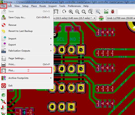
Step 3: Access the Plot Dialog
- In the PCB layout editor, go to “File” > “Plot…” to open the plot dialog window.
Step 4: Configure the Plot Settings
In the plot dialog window, you need to configure various settings to generate the Gerber files.
- Output directory: Choose the folder where you want to save the generated Gerber files.
- Plot format: Select “Gerber” as the plot format.
- Layers to plot: Select the layers you want to include in the Gerber files. Typically, you’ll need to plot the following layers:
- F.Cu (Front Copper)
- B.Cu (Back Copper)
- F.SilkS (Front Silkscreen)
- B.SilkS (Back Silkscreen)
- F.Mask (Front Solder Mask)
- B.Mask (Back Solder Mask)
- Edge.Cuts (Board Outline)
- Plot options: Configure the following plot options:
- Scale: 1:1
- Negative plot: Unchecked
- Exclude PCB edge layer from other layers: Checked
- Use auxiliary axis as origin: Unchecked
- Gerber Options: Click on the “Gerber Options” button to open the Gerber options dialog. Set the following options:
- Format: 4.6 (unit mm)
- Coordinate format: 4.6
- Suppress leading zeros: Unchecked
- Suppress trailing zeros: Checked
- Clear aperture macros: Checked
- Line width: 0.1 mm
Step 5: Generate Drill Files
In addition to the Gerber files, you also need to generate drill files that specify the locations and sizes of the holes in your PCB.
- In the plot dialog window, click on the “Generate Drill Files…” button.
- Configure the following drill file settings:
- Drill units: Millimeters
- Zeros format: Decimal format
- Drill map file format: PostScript
- Drill report format: Report
- Merge PTH and NPTH holes into one file: Checked
- Click “OK” to generate the drill files.
Step 6: Plot the Gerber and Drill Files
- Back in the plot dialog window, click on the “Plot” button to generate the Gerber files.
- Wait for the plotting process to complete. You should see a message indicating that the Gerber files were successfully created.
- Close the plot dialog window.
Step 7: Verify the Generated Files
- Navigate to the output directory you specified earlier.
- Check that all the necessary Gerber and drill files were generated. You should have files with extensions like .gbr, .drl, .rpt, etc.
- Open the Gerber files using a Gerber Viewer to ensure that they match your PCB design. Popular Gerber viewers include:
- GerbView (included with KiCad)
- ViewMate
- CAM350
- Ucamco UcamX
Step 8: Compress and Send the Files to the Manufacturer
- Compress all the generated Gerber and drill files into a single ZIP archive.
- Send the ZIP file to your chosen PCB manufacturer, along with any additional instructions or requirements for your PCB order.
| File Type | Extension | Description |
|---|---|---|
| Copper Layers | .gtl, .gbl | Top and bottom copper layers |
| Solder Mask | .gts, .gbs | Top and bottom solder mask layers |
| Silkscreen | .gto, .gbo | Top and bottom silkscreen layers |
| Board Outline | .gko | PCB outline and cutouts |
| Drill Files | .drl, .rpt | Drill data and report |

Frequently Asked Questions (FAQ)
- What are the most common issues encountered when exporting KiCad PCB to Gerber files?
- Incorrect layer selection
- Improper plot settings
- Missing or incorrect drill files
-
Inconsistencies between Gerber files and original PCB design
-
How can I ensure that my Gerber files are correctly generated?
- Double-check the plot settings and layer selection before generating the files
- Use a Gerber viewer to visually inspect the generated files
-
Compare the Gerber files with your original PCB design to ensure consistency
-
What should I do if my PCB manufacturer reports issues with the Gerber files?
- Ask the manufacturer for specific details about the issues they encountered
- Review your plot settings and make necessary adjustments
-
Regenerate the Gerber files and send them to the manufacturer for verification
-
Can I include additional information or instructions for the PCB manufacturer?
- Yes, you can include a README file or a fabrication drawing with your Gerber files
-
Provide clear instructions on any special requirements, such as PCB Thickness, material, or surface finish
-
How can I learn more about Gerber files and PCB fabrication?
- Consult the KiCad documentation and tutorials
- Visit PCB manufacturing websites and read their guidelines and resources
- Engage with the KiCad community and forums to learn from experienced designers
- Attend workshops or courses on PCB design and fabrication
By following this step-by-step guide and understanding the key concepts behind Gerber files, you’ll be able to successfully export your KiCad PCB designs and have them manufactured with ease. Remember to always double-check your settings, use Gerber viewers for verification, and communicate clearly with your PCB manufacturer to ensure the best results.


Leave a Reply