Table of Contents
- Introduction to PCB Panelization
- Benefits of PCB Panelization
- PCB Panelization Methods
- 3.1. Tab Routing
- 3.2. V-Scoring
- 3.3. Perforated Panels
- 3.4. Rail Panels
- Design Considerations for PCB Panelization
- 4.1. Panel Size and Material
- 4.2. Component Placement and Orientation
- 4.3. Fiducial Markers and Tooling Holes
- 4.4. Breakaway Tabs and Mousebites
- PCB Panelization Best Practices
- 5.1. Panelization Software Tools
- 5.2. Collaboration with PCB Manufacturers
- 5.3. Testing and Quality Control
- Challenges and Limitations of PCB Panelization
- Future Trends in PCB Panelization
- Frequently Asked Questions (FAQ)
- Conclusion
1. Introduction to PCB Panelization
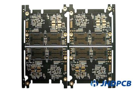
PCB panelization is the process of arranging multiple identical or different PCB designs on a single, larger panel for manufacturing purposes. This approach allows for the simultaneous fabrication and assembly of several PCBs, resulting in increased efficiency and cost-effectiveness. Panelization is particularly beneficial for high-volume production runs and when dealing with small-sized PCBs.
The primary goal of PCB panelization is to maximize the utilization of the available panel space while ensuring that the individual PCBs can be easily separated after the assembly process. This is achieved through various panelization methods, each with its own advantages and considerations.

2. Benefits of PCB Panelization
PCB panelization offers several key benefits to electronics manufacturers and designers:
-
Cost Reduction: By grouping multiple PCBs on a single panel, the overall manufacturing cost per board is reduced. This is because the setup time and material costs are shared across the entire panel, rather than individual boards.
-
Increased Efficiency: Panelization allows for the simultaneous fabrication and assembly of multiple PCBs, which significantly reduces the time required for production. This improved efficiency translates to faster turnaround times and higher throughput.
-
Consistent Quality: When PCBs are panelized, they undergo the same manufacturing processes under identical conditions. This ensures consistent quality across all the boards in the panel, minimizing variations and defects.
-
Simplified Handling: Panelized PCBs are easier to handle during the assembly process, as they can be treated as a single unit. This simplifies pick-and-place operations, soldering, and other assembly steps.
-
Optimized Material Usage: Panelization helps optimize the utilization of the PCB Substrate material, reducing waste and minimizing the environmental impact of the manufacturing process.

3. PCB Panelization Methods
There are several methods used for PCB panelization, each with its own characteristics and suitability for different applications. The choice of panelization method depends on factors such as the PCB design, component placement, and the desired separation technique. Let’s explore some of the most common PCB panelization methods:
3.1. Tab Routing
Tab routing is a popular panelization method that involves connecting individual PCBs with small tabs or “bridges.” These tabs are strategically placed along the edges of the PCBs, allowing them to remain attached to the panel during the manufacturing process. After assembly, the tabs are easily broken or cut to separate the individual boards.
Advantages of tab routing include:
– Simple and cost-effective method
– Suitable for a wide range of PCB designs
– Allows for easy separation of individual boards
Disadvantages:
– Requires additional panel space for the tabs
– May leave visible tab remnants on the board edges after separation
3.2. V-Scoring
V-scoring is a panelization technique that involves creating V-shaped grooves along the edges of the individual PCBs. These grooves are cut partially through the panel thickness, creating a weakened line that allows for easy separation of the boards after assembly. V-scoring is often used for PCBs with irregular shapes or when a clean, smooth edge is required.
Advantages of V-scoring:
– Provides clean, smooth edges after separation
– Suitable for irregular-shaped PCBs
– Minimizes the visible remnants of the panelization process
Disadvantages:
– Requires specialized equipment for V-scoring
– May weaken the structural integrity of the panel during handling
3.3. Perforated Panels
Perforated panels, also known as break-away panels, feature a series of small, closely spaced holes along the edges of the individual PCBs. These perforations create a weakened line that allows for easy separation of the boards after assembly. Perforated panels are commonly used for small-sized PCBs and when a large number of boards need to be panelized.
Advantages of perforated panels:
– Suitable for high-volume production of small PCBs
– Allows for easy separation of individual boards
– Minimizes the panel area required for panelization
Disadvantages:
– May leave visible perforation remnants on the board edges
– Requires precise control of the perforation process to ensure consistent results
3.4. Rail Panels
Rail panels involve attaching individual PCBs to a frame or “rail” that surrounds the perimeter of the panel. The PCBs are connected to the rail using small tabs or breakaway points, which are removed after assembly to separate the boards. Rail panels are often used for larger PCBs or when a more robust panelization solution is required.
Advantages of rail panels:
– Provides a sturdy and stable panel for handling and assembly
– Suitable for larger PCBs and those requiring additional support
– Allows for easy separation of individual boards
Disadvantages:
– Increases the overall panel size and material usage
– May require additional processing steps to remove the rails after assembly

4. Design Considerations for PCB Panelization
When designing PCBs for panelization, several key factors must be considered to ensure a successful manufacturing process and the proper separation of individual boards. These considerations include:
4.1. Panel Size and Material
The choice of panel size and material is crucial for efficient panelization. The panel size should be optimized to accommodate the maximum number of PCBs while leaving sufficient space for panelization features such as tabs, V-scores, or perforations. The material selection should take into account the PCB Thickness, copper weight, and any special requirements such as controlled impedance or high-frequency performance.
Common panel sizes and materials include:
– Standard panel sizes: 18″ x 24″, 21″ x 24″, 24″ x 30″
– Common materials: FR-4, Rogers, Polyimide, Aluminum
4.2. Component Placement and Orientation
When panelizing PCBs, it is essential to consider the placement and orientation of components on the individual boards. Components should be positioned in a way that allows for efficient assembly and minimizes the risk of damage during the panelization process. Additionally, the orientation of the components should be consistent across all the boards in the panel to facilitate automated assembly.
Guidelines for component placement and orientation:
– Maintain sufficient clearance between components and board edges
– Avoid placing tall components near the edges of the panel
– Ensure consistent Component Orientation across all boards in the panel
4.3. Fiducial Markers and Tooling Holes
Fiducial markers and tooling holes are essential features in PCB panelization that aid in the alignment and registration of the panel during the manufacturing process. Fiducial markers are small, precisely placed marks on the panel that serve as reference points for automated assembly equipment. Tooling holes, on the other hand, are used to securely hold the panel in place during fabrication and assembly.
Considerations for fiducial markers and tooling holes:
– Place fiducial markers at strategic locations on the panel
– Ensure adequate clearance around fiducial markers and tooling holes
– Follow the manufacturer’s guidelines for fiducial marker and tooling Hole Sizes
4.4. Breakaway Tabs and Mousebites
Breakaway tabs and mousebites are features used in PCB panelization to facilitate the separation of individual boards after assembly. Breakaway tabs are small, connecting bridges between the PCBs and the panel frame, which are easily broken or cut to detach the boards. Mousebites, also known as perforations, are series of small holes that create a weakened line along which the boards can be separated.
Design considerations for breakaway tabs and mousebites:
– Determine the appropriate size and spacing of breakaway tabs and mousebites
– Ensure sufficient mechanical strength to hold the boards during assembly
– Consider the ease of separation and the potential for leaving visible remnants on the board edges
5. PCB Panelization Best Practices
To achieve optimal results in PCB panelization, following best practices and leveraging the right tools and collaborations is essential. Here are some key best practices to consider:
5.1. Panelization Software Tools
Using specialized panelization software tools can significantly streamline the design and preparation process for PCB panelization. These tools offer features such as automatic panel layout generation, design rule checks, and panelization simulations. Some popular PCB panelization software tools include:
- Altium Designer
- Cadence Allegro
- Mentor Graphics Xpedition
- Zuken CR-8000
5.2. Collaboration with PCB Manufacturers
Collaborating closely with PCB manufacturers is crucial for successful panelization. Manufacturers have extensive experience and knowledge of panelization techniques, material requirements, and process limitations. By engaging with manufacturers early in the design process, potential issues can be identified and resolved, ensuring a smooth and efficient production process.
Best practices for collaboration with PCB manufacturers:
– Communicate panelization requirements and preferences early in the design process
– Provide detailed documentation, including panel layouts and design files
– Seek feedback and guidance from manufacturers on panelization methods and design optimization
5.3. Testing and Quality Control
Implementing rigorous testing and quality control measures is essential to ensure the reliability and functionality of panelized PCBs. This includes visual inspections, electrical testing, and mechanical stress tests to verify the integrity of the panelization features and the individual boards.
Quality control measures for panelized PCBs:
– Perform visual inspections to identify any defects or irregularities in the panelization features
– Conduct electrical testing to verify the functionality and performance of the individual boards
– Perform mechanical stress tests to assess the strength and durability of the panelization features
6. Challenges and Limitations of PCB Panelization
While PCB panelization offers numerous benefits, it is important to be aware of the challenges and limitations associated with this process. Some of the key challenges include:
-
Design Complexity: Panelization adds an extra layer of complexity to the PCB design process, requiring careful consideration of panelization features, component placement, and board layout.
-
Material Waste: Panelization inevitably results in some material waste, as the space between individual boards and the panelization features is not utilized for functional circuitry.
-
Separation Challenges: Depending on the panelization method used, separating individual boards from the panel can be challenging and may require specialized equipment or manual intervention.
-
Compatibility Issues: Some PCB designs may not be suitable for certain panelization methods due to their size, shape, or component placement, requiring alternative approaches or modifications.
7. Future Trends in PCB Panelization
As the electronics industry continues to evolve, PCB panelization techniques and technologies are also advancing to meet the changing demands. Some of the future trends in PCB panelization include:
-
Automated Panelization Software: The development of more sophisticated and intelligent panelization software tools that can automatically optimize panel layouts, minimize material waste, and ensure design rule compliance.
-
Advanced Materials: The adoption of advanced PCB materials with improved mechanical and electrical properties, enabling more efficient and reliable panelization processes.
-
Flexible and Stretchable PCBs: The increasing demand for flexible and stretchable PCBs in wearable electronics and IoT devices is driving the development of new panelization techniques specifically tailored for these applications.
-
Sustainable Panelization: The focus on environmentally friendly and sustainable manufacturing practices is leading to the exploration of eco-friendly panelization methods and materials that minimize waste and reduce the carbon footprint.
8. Frequently Asked Questions (FAQ)
-
Q: What is the purpose of PCB panelization?
A: The purpose of PCB panelization is to group multiple PCB designs onto a single panel for efficient fabrication and assembly, reducing manufacturing costs and improving overall throughput. -
Q: What are the most common PCB panelization methods?
A: The most common PCB panelization methods include tab routing, V-scoring, perforated panels, and rail panels. Each method has its own advantages and considerations based on the PCB design and manufacturing requirements. -
Q: How does PCB panelization affect the design process?
A: PCB panelization adds an extra layer of complexity to the design process, requiring careful consideration of panelization features, component placement, and board layout. Designers must work closely with manufacturers to ensure optimal panelization results. -
Q: What are the benefits of using panelization software tools?
A: Panelization software tools streamline the design and preparation process for PCB panelization by offering features such as automatic panel layout generation, design rule checks, and panelization simulations. These tools help optimize panel utilization and minimize potential issues. -
Q: How can I ensure the quality and reliability of panelized PCBs?
A: To ensure the quality and reliability of panelized PCBs, implement rigorous testing and quality control measures, including visual inspections, electrical testing, and mechanical stress tests. Collaborate closely with PCB manufacturers and follow best practices for panelization design and production.
9. Conclusion
PCB panelization is a crucial process in electronics manufacturing that enables the efficient fabrication and assembly of multiple PCBs on a single panel. By understanding the various panelization methods, design considerations, and best practices, designers and manufacturers can optimize their production processes, reduce costs, and improve overall product quality.
As the electronics industry continues to evolve, staying informed about the latest trends and advancements in PCB panelization is essential for staying competitive and meeting the ever-changing demands of the market. By embracing new technologies, materials, and sustainable practices, the PCB panelization process will continue to play a vital role in driving innovation and growth in the electronics sector.


Leave a Reply