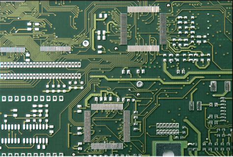
What are Multilayer PCBs?
Multilayer PCBs, also known as multilayer printed circuit boards, are a type of PCB that consists of multiple layers of conductive material, typically copper, separated by insulating layers. These layers are laminated together to form a single, compact board that can accommodate complex circuits and high component density. Multilayer PCBs offer several advantages over single-layer and double-layer PCBs, making them essential for a wide range of applications, from consumer electronics to aerospace and military systems.
Advantages of Multilayer PCBs
- Increased circuit density
- Improved signal integrity
- Better heat dissipation
- Enhanced mechanical strength
- Reduced electromagnetic interference (EMI)
How are Multilayer PCBs Manufactured?
The manufacturing process for multilayer PCBs involves several steps, each requiring precision and careful control to ensure the final product meets the desired specifications.
Step 1: Design and Layout
The first step in manufacturing a multilayer PCB is to create a detailed design and layout using specialized PCB design software. This process involves determining the number of layers required, the placement of components, and the routing of traces between components. The design must also take into account factors such as signal integrity, power distribution, and thermal management.
Step 2: Layer Preparation
Once the design is finalized, the individual layers of the PCB are prepared. This involves printing the conductive traces onto thin sheets of insulating material, such as FR-4, using a photolithographic process. The copper traces are etched onto the substrate using a chemical process, and any unnecessary copper is removed.
Step 3: Lamination
The prepared layers are then stacked and aligned according to the design specifications. The stack is then laminated together under high pressure and temperature, typically using a hydraulic press. This process bonds the layers together and ensures that the conductive traces on each layer are properly aligned.
Step 4: Drilling and Plating
After lamination, holes are drilled through the board to accommodate through-hole components and to create vias, which are used to connect traces on different layers. The holes are then plated with copper to ensure electrical continuity between layers.
Step 5: Surface Finishing
The final step in the manufacturing process is to apply a surface finish to the PCB. This can include applying a solder mask to protect the copper traces, adding silkscreen labels for component placement, and plating exposed copper with a protective coating, such as gold or nickel.

Types of Multilayer PCBs
Multilayer PCBs can be categorized based on the number of layers they contain and the specific manufacturing techniques used.
4-Layer PCBs
4-layer PCBs are the most common type of multilayer PCB and are widely used in consumer electronics, telecommunications equipment, and industrial control systems. They consist of two inner layers, typically used for power and ground planes, and two outer layers for signal routing.
6-Layer and 8-Layer PCBs
As the complexity of electronic systems increases, so does the need for PCBs with more layers. 6-layer and 8-layer PCBs offer increased routing density and better signal integrity compared to 4-layer boards. They are commonly used in high-speed digital systems, such as computer motherboards and network switches.
High-Density Interconnect (HDI) PCBs
HDI PCBs are a specialized type of multilayer PCB that features very fine traces and small vias, allowing for even greater component density and signal integrity. HDI PCBs often incorporate microvias, which are small, laser-drilled holes that connect adjacent layers, and buried vias, which are used to connect inner layers without penetrating the outer layers. HDI PCBs are used in high-performance applications, such as smartphones, wearable devices, and medical implants.

Designing Multilayer PCBs
Designing multilayer PCBs requires careful consideration of several factors to ensure optimal performance and manufacturability.
Signal Integrity
One of the primary challenges in designing multilayer PCBs is maintaining signal integrity, particularly in high-speed digital systems. Factors such as crosstalk, impedance mismatch, and signal reflections can degrade signal quality and lead to system failures. To mitigate these issues, designers must carefully route traces, control trace geometry, and use appropriate termination techniques.
Power Distribution
Proper power distribution is essential for ensuring the reliable operation of electronic systems. In multilayer PCBs, dedicated power and ground planes are often used to provide low-impedance, low-noise power distribution to components. Designers must also consider factors such as voltage drop, current carrying capacity, and thermal management when designing power distribution networks.
Stackup Design
The arrangement of layers in a multilayer PCB, known as the stackup, plays a critical role in determining the board’s electrical and mechanical properties. Designers must carefully select the number and arrangement of layers based on the specific requirements of the application. Factors such as dielectric constant, layer thickness, and copper weight must be considered to ensure optimal performance.
Manufacturability
Designing multilayer PCBs for manufacturability is essential for ensuring reliable, cost-effective production. Designers must adhere to established design rules and guidelines, such as minimum trace width and spacing, hole size and spacing, and clearance requirements. Collaborating with the PCB manufacturer throughout the design process can help identify and resolve potential manufacturing issues early on.

Applications of Multilayer PCBs
Multilayer PCBs are used in a wide range of applications across various industries, from consumer electronics to aerospace and defense.
| Industry | Applications |
|---|---|
| Consumer Electronics | Smartphones, tablets, laptops, gaming systems, wearable devices |
| Automotive | Engine control units, infotainment systems, advanced driver assistance systems (ADAS) |
| Aerospace and Defense | Avionics, radar systems, satellite communications, Military Electronics |
| Medical | Imaging systems, diagnostic equipment, implantable devices, surgical instruments |
| Industrial | Automation and control systems, power electronics, robotics, IoT devices |
| Telecommunications | Network switches, routers, base stations, fiber optic equipment |
Frequently Asked Questions (FAQ)
1. What is the difference between a multilayer PCB and a Single-Layer PCB?
A single-layer PCB has conductive traces on only one side of the board, while a multilayer PCB has multiple layers of conductive traces separated by insulating layers. Multilayer PCBs offer increased circuit density, improved signal integrity, and better thermal management compared to single-layer PCBs.
2. How many layers can a multilayer PCB have?
Multilayer PCBs can have anywhere from 4 to over 50 layers, depending on the complexity of the circuit and the specific application requirements. The most common multilayer PCBs have 4, 6, or 8 layers, while high-density PCBs can have 12 or more layers.
3. What materials are used in the construction of multilayer PCBs?
The most common base material used in multilayer PCBs is FR-4, a glass-reinforced epoxy laminate. Other materials, such as polyimide and PTFE, may be used for high-frequency or high-temperature applications. The conductive layers are typically made of copper, while the insulating layers can be made of various materials, such as prepreg or adhesive film.
4. What are the advantages of using HDI PCBs?
HDI (High-Density Interconnect) PCBs offer several advantages over traditional multilayer PCBs, including increased component density, improved signal integrity, and reduced board size and weight. HDI PCBs use smaller vias and finer traces, allowing for more compact designs and higher performance in high-speed digital systems.
5. How can I ensure my multilayer PCB design is manufacturable?
To ensure your multilayer PCB design is manufacturable, follow established design rules and guidelines provided by your PCB manufacturer. This includes adhering to minimum trace width and spacing, hole size and spacing, and clearance requirements. Collaborate with your manufacturer throughout the design process to identify and resolve potential manufacturing issues early on.
Conclusion
Multilayer PCBs are essential components in a wide range of electronic systems, offering increased circuit density, improved signal integrity, and better thermal management compared to single-layer and double-layer PCBs. Understanding the manufacturing process, types of multilayer PCBs, and key design considerations is crucial for creating reliable, high-performance electronic devices.
As electronic systems continue to become more complex and compact, the demand for advanced multilayer PCB technologies, such as HDI PCBs, will only continue to grow. By staying up-to-date with the latest developments in multilayer PCB design and manufacturing, engineers and designers can create innovative solutions that push the boundaries of what is possible in the world of electronics.


Leave a Reply