Introduction to Single-Layer PCBs
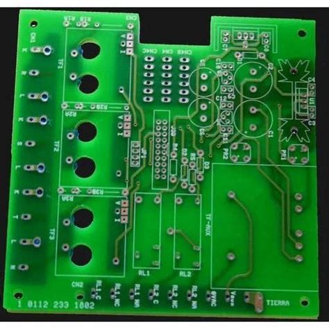
A Single-Layer PCB (Printed Circuit Board) is the simplest and most basic type of PCB. As the name suggests, it consists of only one layer of substrate or base material, with conductive copper traces printed on one side. The other side of the board is left bare or covered with a solder mask for protection.
Single-layer PCBs are widely used in simple electronic devices and projects due to their low cost, ease of design and manufacturing, and reliability for basic circuits. They are ideal for prototyping, hobbyist projects, and mass production of simple devices.
Advantages of Single-Layer PCBs
- Cost-effective: Single-layer PCBs are the most affordable type of PCB due to their simple design and manufacturing process.
- Easy to design: Designing a single-layer PCB is relatively straightforward, as there are no complex routing or layer alignment issues to consider.
- Quick turnaround time: Due to their simplicity, single-layer PCBs can be manufactured quickly, making them ideal for rapid prototyping and short production runs.
- Reliable for simple circuits: Single-layer PCBs are well-suited for basic electronic circuits with few components and minimal complexity.
Disadvantages of Single-Layer PCBs
- Limited circuit complexity: As there is only one conductive layer, single-layer PCBs are not suitable for complex circuits with many components or intricate routing requirements.
- Larger board size: To accommodate all the necessary components and traces, single-layer PCBs may require a larger board size compared to multi-layer PCBs.
- Potential for electromagnetic interference: With all components and traces on one side, single-layer PCBs are more susceptible to electromagnetic interference (EMI) and noise.
Single-Layer PCB Manufacturing Process
The manufacturing process for single-layer PCBs typically involves the following steps:
-
Design: The PCB design is created using electronic design automation (EDA) software, which generates the necessary Gerber files for manufacturing.
-
Copper cladding: A thin layer of copper foil is bonded to the substrate material, typically FR-4 (a glass-reinforced epoxy laminate).
-
Printing: The PCB design is printed onto the copper-clad substrate using a photoresist process. The photoresist is exposed to UV light through a photomask, which hardens the exposed areas.
-
Etching: The unexposed photoresist is removed, and the exposed copper is etched away using a chemical solution, leaving only the desired conductive traces.
-
Drilling: Holes are drilled through the board for component leads and vias (if required).
-
Solder mask application (optional): A solder mask is applied to the board to protect the copper traces and prevent solder bridging.
-
Silkscreen printing (optional): A silkscreen layer is printed onto the board to add component labels, logos, and other markings.
-
Surface finish (optional): A surface finish, such as HASL (Hot Air Solder Leveling) or ENIG (Electroless Nickel Immersion Gold), is applied to the exposed copper to prevent oxidation and enhance solderability.
-
Cutting and routing: The manufactured panel is cut and routed into individual PCBs.
-
Quality control: The finished PCBs undergo a quality control process to ensure they meet the required specifications and functionality.

Designing Single-Layer PCBs
When designing a single-layer PCB, consider the following guidelines:
-
Component placement: Arrange components logically and efficiently to minimize trace lengths and crossovers. Place related components close together and consider the flow of signals through the circuit.
-
Trace width and spacing: Ensure that trace widths are appropriate for the current carrying requirements of the circuit. Maintain adequate spacing between traces to prevent short circuits and minimize electromagnetic interference.
-
Grounding: Provide a solid ground plane on the PCB to improve signal integrity and reduce noise. Use wide traces or a copper pour for the ground connection.
-
Solder mask and silkscreen: Include a solder mask to protect the copper traces and prevent solder bridging. Use silkscreen labels to clearly identify components and their orientations.
-
Design rules check (DRC): Run a DRC on the PCB design to ensure it meets the manufacturing specifications and design guidelines provided by the PCB fabricator.

Applications of Single-Layer PCBs
Single-layer PCBs are used in a variety of simple electronic devices and applications, such as:
- Consumer electronics: Remote controls, calculators, simple toys, and appliances.
- Automotive electronics: Simple control modules, lighting circuits, and sensor interfaces.
- Hobbyist projects: Arduino shields, breadboard adapters, and simple sensor circuits.
- Educational kits: Electronic learning kits and STEM projects for students.
- Prototyping: Quick and affordable prototypes for proof-of-concept designs.

Comparing Single-Layer PCBs to Other PCB Types
Single-layer PCBs are the simplest and most affordable type of PCB, but they have limitations in terms of circuit complexity and board size. Here’s a comparison of single-layer PCBs to other common PCB types:
| PCB Type | Layers | Complexity | Cost | Applications |
|---|---|---|---|---|
| Single-layer | 1 | Low | Low | Simple devices, prototyping |
| Double-layer | 2 | Medium | Medium | More complex devices, power and ground planes |
| Multi-layer | 4+ | High | High | High-speed devices, dense designs, EMI reduction |
| Flexible | Varies | Low to High | High | Wearables, compact devices, interconnects |
| Rigid-Flex | Varies | High | Very High | Complex devices, 3D packaging, reliability |
Frequently Asked Questions (FAQ)
1. What is the minimum trace width and spacing for a single-layer PCB?
The minimum trace width and spacing for a single-layer PCB depend on the PCB fabricator’s capabilities and the specific design requirements. Typically, a minimum trace width of 0.15mm (6mil) and a minimum spacing of 0.15mm (6mil) are achievable for most PCB Manufacturers. However, it’s essential to consult with your chosen PCB fabricator for their specific design guidelines.
2. Can single-layer PCBs have through-hole components?
Yes, single-layer PCBs can accommodate through-hole components. The component leads are inserted through drilled holes in the board and soldered on the opposite side. However, through-hole components occupy more space than surface-mount components, which can limit the circuit complexity and density on a single-layer PCB.
3. Are single-layer PCBs suitable for high-frequency circuits?
Single-layer PCBs are generally not recommended for high-frequency circuits due to their limited ability to control impedance and manage electromagnetic interference (EMI). For high-frequency applications, multi-layer PCBs with dedicated power and ground planes and controlled impedance traces are more suitable.
4. How do I choose the right substrate material for my single-layer PCB?
The most common substrate material for single-layer PCBs is FR-4, a glass-reinforced epoxy laminate. FR-4 offers good mechanical stability, electrical insulation, and heat resistance. For high-frequency or specialized applications, other substrate materials like Rogers, Teflon, or Polyimide may be more appropriate. Consider the electrical, thermal, and mechanical requirements of your design when selecting the substrate material.
5. Can I design and manufacture a single-layer PCB at home?
Yes, it is possible to design and manufacture simple single-layer PCBs at home using a variety of methods, such as toner transfer, photo etching, or CNC milling. However, home-made PCBs may not have the same quality, reliability, and precision as professionally manufactured boards. For critical or complex designs, it’s recommended to use a professional PCB Fabrication service.
Conclusion
Single-layer PCBs are an essential part of the electronics industry, offering a cost-effective and reliable solution for simple circuit designs and prototyping. By understanding the advantages, limitations, and design considerations of single-layer PCBs, engineers and hobbyists can effectively utilize them in their projects.
As technology advances and circuit complexity increases, single-layer PCBs may not always be the optimal choice. However, they will continue to play a vital role in entry-level electronics, educational projects, and rapid prototyping. By mastering the art of single-layer PCB design, you can create successful and functional electronic devices while minimizing costs and development time.


Leave a Reply