Introduction to Tenting Via in PCB Fabrication
Printed Circuit Board (PCB) fabrication is a complex process that involves several steps, each of which plays a crucial role in ensuring the quality and reliability of the final product. One of the essential techniques used in PCB fabrication is tenting via, which is a method of covering the Via holes on a PCB with a layer of solder mask.
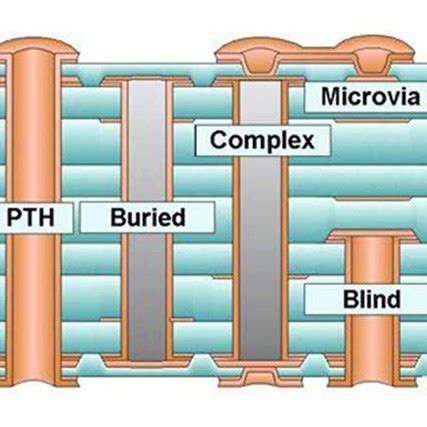
What is a Via?
Before we dive into the details of tenting via, let’s first understand what a via is. A via is a small hole drilled through a PCB that allows electrical connections to be made between different layers of the board. Vias are essential in PCB Design as they enable the routing of signals and power between different layers, thus allowing for more complex and compact designs.
Why is Tenting Via Important?
Tenting via is an important technique in PCB fabrication for several reasons:
-
Protection from Contaminants: Tenting via helps to protect the via holes from contaminants such as dust, dirt, and moisture, which can cause short circuits and other issues.
-
Improved Insulation: By covering the via holes with a layer of solder mask, tenting via improves the insulation between the different layers of the PCB, thus reducing the risk of electrical interference and signal crosstalk.
-
Enhanced Mechanical Strength: Tenting via also provides additional mechanical strength to the PCB, as the solder mask layer helps to reinforce the via holes and prevent them from breaking or cracking under stress.
-
Improved Aesthetics: Tenting via can also improve the aesthetics of the PCB, as it creates a smooth and uniform surface finish that is free from exposed via holes.
Types of Tenting Via
There are two main types of tenting via used in PCB fabrication:
1. Partial Tenting Via
Partial tenting via is a technique where only a portion of the via hole is covered with solder mask, leaving the center of the via exposed. This method is often used when the via needs to be accessible for testing or debugging purposes.
2. Full Tenting Via
Full tenting via, also known as complete tenting via, is a technique where the entire via hole is covered with solder mask, leaving no exposed metal. This method provides the highest level of protection and insulation for the via holes.

Tenting Via Process
The tenting via process typically involves the following steps:
-
Drilling: The first step in the tenting via process is to drill the via holes into the PCB using a CNC drill machine.
-
Plating: After drilling, the via holes are plated with a conductive material, such as copper, to create an electrical connection between the different layers of the PCB.
-
Solder Mask Application: Next, a layer of solder mask is applied to the surface of the PCB, covering the via holes and other exposed areas.
-
Exposure and Developing: The solder mask layer is then exposed to UV light through a photomask, which hardens the areas that will remain on the PCB. The unexposed areas are then removed using a developing solution.
-
Curing: Finally, the PCB is heated to cure the solder mask layer, creating a hard and durable surface finish.

Advantages of Tenting Via
Tenting via offers several advantages over other methods of via protection, such as filling or plugging:
-
Cost-effective: Tenting via is a cost-effective method of via protection, as it does not require any additional materials or processing steps beyond the standard solder mask application.
-
Reliable: Tenting via provides a reliable and durable method of via protection, as the solder mask layer is designed to withstand harsh environmental conditions and mechanical stress.
-
Versatile: Tenting via can be used on a wide range of PCB designs, from simple single-layer boards to complex multi-layer designs.
-
Improved Signal Integrity: By providing a smooth and uniform surface finish, tenting via can help to improve signal integrity and reduce signal loss.

Disadvantages of Tenting Via
While tenting via offers many benefits, there are also some potential disadvantages to consider:
-
Limited Via Size: Tenting via may not be suitable for very small via holes, as the solder mask layer may not be able to fully cover the hole without blocking it entirely.
-
Reduced Thermal Conductivity: The solder mask layer used in tenting via can reduce the thermal conductivity of the via holes, which may be a concern for high-power applications.
-
Potential for Voids: If the solder mask layer is not applied properly, there is a risk of voids forming around the via holes, which can lead to reliability issues.
Best Practices for Tenting Via
To ensure the best results when using tenting via in PCB fabrication, there are several best practices to follow:
-
Choose the Right Solder Mask: Select a high-quality solder mask material that is compatible with your PCB design and manufacturing process.
-
Use Proper Via Size: Ensure that the via holes are sized appropriately for the tenting via process, taking into account the thickness of the solder mask layer.
-
Control the Solder Mask Thickness: Carefully control the thickness of the solder mask layer to ensure complete coverage of the via holes without blocking them entirely.
-
Optimize the Exposure and Developing Process: Fine-tune the exposure and developing process to ensure that the solder mask layer is fully cured and free from defects.
-
Conduct Thorough Testing: Conduct thorough testing and inspection of the PCB after the tenting via process to ensure that the via holes are fully protected and functioning properly.
FAQ
1. What is the difference between tenting via and filling via?
Tenting via involves covering the via holes with a layer of solder mask, while filling via involves filling the via holes with a conductive material, such as copper or conductive epoxy. Tenting via is typically more cost-effective and versatile, while filling via provides better thermal conductivity and can be used for high-power applications.
2. Can tenting via be used on both through-hole and blind/buried vias?
Yes, tenting via can be used on both through-hole and blind/buried vias. However, the process may need to be adjusted slightly depending on the specific type of via being used.
3. How does tenting via affect the impedance of the PCB?
Tenting via can affect the impedance of the PCB by adding a layer of dielectric material (the solder mask) around the via holes. This can change the capacitance and inductance of the via, which can impact the overall impedance of the PCB. However, these effects can be minimized through careful design and material selection.
4. What is the typical thickness of the solder mask layer used in tenting via?
The typical thickness of the solder mask layer used in tenting via ranges from 0.5 to 2 mils (0.0127 to 0.0508 mm). The specific thickness will depend on the PCB design, manufacturing process, and solder mask material being used.
5. Can tenting via be used in High-Frequency PCB designs?
Yes, tenting via can be used in high-frequency PCB designs, but care must be taken to ensure that the solder mask material and thickness are chosen appropriately to minimize any impact on signal integrity. In some cases, other via protection methods, such as filling or plugging, may be more suitable for high-frequency applications.
Conclusion
Tenting via is a critical technique used in PCB fabrication to protect via holes from contaminants, improve insulation and mechanical strength, and enhance the overall aesthetics of the PCB. By understanding the different types of tenting via, the advantages and disadvantages of the process, and the best practices for implementation, PCB designers and manufacturers can ensure the highest level of quality and reliability in their products. As PCB technology continues to evolve, tenting via will likely remain an essential tool in the fabrication process, helping to enable the next generation of electronic devices and systems.


Leave a Reply