Introduction to Via holes
In the world of printed circuit boards (PCBs), via holes play a crucial role in establishing electrical connections between different layers of a multi-layer PCB. These small, conductive pathways allow signals and power to travel vertically through the board, enabling complex circuits to be designed and manufactured in a compact and efficient manner. This article will delve into the intricacies of via holes, exploring their types, manufacturing processes, design considerations, and their significance in modern electronics.
What is a Via Hole?
A via hole, simply put, is a small hole drilled through a PCB that is subsequently filled or coated with a conductive material, typically copper. These conductive holes serve as interconnects between different layers of a multi-layer PCB, allowing electrical signals and power to pass through the board vertically. Via holes are essential in PCB design as they enable the creation of complex, high-density circuits by utilizing the available space efficiently.
Types of Via Holes
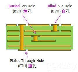
There are several types of via holes used in PCB design, each serving a specific purpose and having its own characteristics. The most common types include:
-
Through Hole Via: These via holes extend through the entire thickness of the PCB, connecting all layers from top to bottom. They are the most basic and commonly used type of via holes.
-
Blind Via: Blind via holes start from either the top or bottom layer of the PCB and terminate at an internal layer, without extending through the entire board thickness. They are used to connect an outer layer to one or more inner layers.
-
Buried Via: Buried via holes are located entirely within the internal layers of a PCB, connecting two or more inner layers without extending to the outer layers. They are used to create connections between inner layers without using space on the outer layers.
-
Microvia: Microvias are small, laser-drilled via holes with diameters typically less than 150 microns. They are used in high-density PCB designs to create fine-pitch interconnects and are often found in HDI (High-Density Interconnect) PCBs.
| Via Type | Description |
|---|---|
| Through Hole | Extends through the entire PCB Thickness, connecting all layers |
| Blind | Starts from an outer layer and terminates at an internal layer |
| Buried | Located entirely within internal layers, connecting inner layers |
| Microvia | Small, laser-drilled via holes with diameters less than 150 microns |
Manufacturing Process of Via Holes
The manufacturing process of via holes involves several steps to ensure proper electrical conductivity and reliability. The basic steps include:
-
Drilling: Via holes are drilled into the PCB substrate using mechanical drilling or laser drilling techniques. The choice of drilling method depends on the size, type, and quantity of via holes required.
-
Deburring and Cleaning: After drilling, the via holes are deburred to remove any rough edges or debris. The holes are then cleaned to ensure proper adhesion of the conductive material.
-
Plating: The via holes are plated with a conductive material, usually copper, through an electroplating process. This step creates a conductive pathway along the walls of the via holes, allowing electrical signals to pass through.
-
Filling (optional): In some cases, via holes may be filled with a non-conductive material, such as epoxy, to improve the structural integrity of the PCB or to create a smooth surface for subsequent layers.

Design Considerations for Via Holes
When designing a PCB, several factors must be considered to ensure the proper functioning and reliability of via holes. Some key design considerations include:
1. Via Hole Size and Placement
The size and placement of via holes are crucial aspects of PCB design. The diameter of the via hole should be large enough to accommodate the required current carrying capacity while maintaining the necessary spacing between adjacent via holes and other components. The placement of via holes should also consider the signal integrity, as improper placement can lead to signal distortion, crosstalk, and electromagnetic interference (EMI).
2. Aspect Ratio
The aspect ratio of a via hole refers to the ratio of its depth to its diameter. A higher aspect ratio indicates a deeper and narrower via hole, which can be more challenging to manufacture and plate properly. It is essential to consider the aspect ratio when designing via holes to ensure that they can be reliably manufactured and function as intended.
3. Current Carrying Capacity
Via holes must be designed to handle the required current carrying capacity of the circuits they connect. The current carrying capacity depends on various factors, such as the via hole diameter, plating thickness, and the temperature rise allowed in the board. Designers must calculate the appropriate via hole size and plating thickness to ensure that the via holes can handle the expected current without overheating or failing.
4. Signal Integrity
Via holes can have a significant impact on signal integrity, particularly in high-speed and high-frequency applications. The transition from a horizontal trace to a vertical via hole can cause impedance mismatches, reflections, and signal distortion. To minimize these effects, designers can use techniques such as via shielding, ground vias, and controlled impedance via holes.
5. Manufacturing Constraints
PCB designers must also consider the manufacturing constraints when designing via holes. Different PCB manufacturers may have varying capabilities in terms of via hole sizes, aspect ratios, and minimum spacing requirements. It is essential to consult with the manufacturer early in the design process to ensure that the via holes can be reliably manufactured and meet the required specifications.

Applications of Via Holes in Modern Electronics
Via holes are essential components in a wide range of modern electronic applications, from consumer devices to industrial equipment and aerospace systems. Some common applications include:
1. High-Density Interconnect (HDI) PCBs
HDI PCBs utilize via holes, particularly microvias, to create high-density interconnects between layers. These PCBs are commonly used in smartphones, tablets, and other compact electronic devices that require a large number of components and connections in a small form factor.
2. Multilayer PCBs
Multilayer PCBs rely heavily on via holes to establish connections between the various layers of the board. These PCBs are used in a wide range of applications, from consumer electronics to industrial control systems and medical devices.
3. High-Speed Digital Circuits
Via holes play a critical role in high-speed digital circuits, such as those found in computer processors, network equipment, and telecommunications systems. Properly designed via holes help maintain signal integrity and minimize signal distortion in these high-frequency applications.
4. Power Electronics
In power electronics applications, via holes are used to connect power planes and distribute power throughout the PCB. These via holes must be designed to handle the required current carrying capacity and minimize resistive losses to ensure efficient and reliable power delivery.

Frequently Asked Questions (FAQ)
-
What is the difference between a through hole via and a blind via?
A through hole via extends through the entire thickness of the PCB, connecting all layers from top to bottom. In contrast, a blind via starts from either the top or bottom layer and terminates at an internal layer, without extending through the entire board thickness. -
What is the purpose of Via Filling?
Via filling is the process of filling a via hole with a non-conductive material, such as epoxy. This is done to improve the structural integrity of the PCB, create a smooth surface for subsequent layers, or to prevent the entrapment of air or gases during the assembly process. -
How does the aspect ratio affect the manufacturability of via holes?
The aspect ratio of a via hole is the ratio of its depth to its diameter. A higher aspect ratio indicates a deeper and narrower via hole, which can be more challenging to manufacture and plate properly. PCB designers must consider the aspect ratio to ensure that via holes can be reliably manufactured and function as intended. -
What are microvias, and why are they used in HDI PCBs?
Microvias are small, laser-drilled via holes with diameters typically less than 150 microns. They are used in high-density PCB designs, particularly in HDI PCBs, to create fine-pitch interconnects between layers. Microvias enable the creation of compact, high-density circuits in a small form factor. -
How can via holes impact signal integrity in high-speed digital circuits?
Via holes can have a significant impact on signal integrity in high-speed digital circuits. The transition from a horizontal trace to a vertical via hole can cause impedance mismatches, reflections, and signal distortion. To minimize these effects, designers can use techniques such as via shielding, ground vias, and controlled impedance via holes.
Conclusion
Via holes are essential components in modern PCB design, enabling the creation of complex, high-density circuits in a compact and efficient manner. Understanding the types, manufacturing processes, design considerations, and applications of via holes is crucial for PCB designers and engineers working in various industries.
By carefully considering factors such as via hole size, placement, aspect ratio, current carrying capacity, signal integrity, and manufacturing constraints, designers can create reliable and high-performance PCBs that meet the demands of today’s electronic devices and systems.
As technology continues to advance and the demand for smaller, faster, and more powerful electronic devices grows, the importance of via holes in PCB design will only continue to increase. By staying up-to-date with the latest technologies, design techniques, and manufacturing processes, PCB designers and engineers can ensure that they are creating cutting-edge products that meet the needs of their customers and end-users.


Leave a Reply