Introduction to High-Frequency PCB
In today’s fast-paced world of electronics, the demand for high-speed signal transmission has never been greater. From telecommunications to aerospace, the need for reliable and efficient circuits that can handle high frequencies is paramount. This is where High-Frequency Printed Circuit Boards (PCBs) come into play.
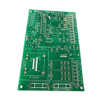
High-Frequency PCBs are specially designed to handle signals with frequencies ranging from a few hundred megahertz (MHz) to several gigahertz (GHz). These PCBs are engineered to minimize signal loss, crosstalk, and electromagnetic interference (EMI), ensuring that the signals are transmitted with high fidelity and minimal distortion.
What Makes High-Frequency PCBs Different?
High-Frequency PCBs differ from traditional PCBs in several key aspects. First and foremost, they are designed to handle much higher frequencies than their conventional counterparts. This requires the use of special materials, such as low-loss dielectrics and high-conductivity copper, to minimize signal attenuation and distortion.
Another critical aspect of High-Frequency PCBs is their layout and routing. The traces on these PCBs must be carefully designed to maintain a consistent impedance throughout the circuit. This is achieved through the use of controlled impedance traces, which are designed to match the impedance of the components and devices connected to the PCB.
Additionally, High-Frequency PCBs often incorporate advanced features such as buried and blind vias, which help to minimize the length of the signal paths and reduce the overall size of the PCB.
Applications of High-Frequency PCB
High-Frequency PCBs find applications in a wide range of industries and sectors. Some of the most common applications include:
Telecommunications
In the telecommunications industry, High-Frequency PCBs are used in a variety of devices, such as mobile phones, base stations, and satellite communications systems. These PCBs are essential for ensuring that the signals are transmitted and received with high fidelity, even over long distances.
Aerospace and Defense
In the aerospace and defense sectors, High-Frequency PCBs are used in radar systems, avionics, and other mission-critical applications. These PCBs must be able to withstand extreme temperatures, vibrations, and other harsh environmental conditions while providing reliable and accurate signal transmission.
Medical Devices
High-Frequency PCBs are also used in various medical devices, such as imaging systems, patient monitoring equipment, and diagnostic tools. These PCBs must meet stringent regulatory requirements and provide high levels of accuracy and reliability to ensure patient safety.
Automotive Electronics
In the automotive industry, High-Frequency PCBs are used in advanced driver assistance systems (ADAS), infotainment systems, and other electronic components. As vehicles become increasingly connected and autonomous, the demand for high-speed, reliable signal transmission continues to grow.

Designing High-Frequency PCB
Designing a High-Frequency PCB requires a deep understanding of the principles of high-speed signal transmission and the various factors that can impact signal integrity. Some of the key considerations when designing a High-Frequency PCB include:
Material Selection
The choice of materials is critical when designing a High-Frequency PCB. The dielectric material must have a low loss tangent and a stable dielectric constant over the desired frequency range. Common materials used in High-Frequency PCBs include Rogers, Isola, and Taconic.
The copper used for the traces and planes must also be of high quality and have a smooth surface finish to minimize skin effect losses. Many High-Frequency PCBs use a special type of copper called low-profile copper (LPC), which has a smoother surface than traditional electrodeposited copper (EDC).
Controlled Impedance
Maintaining a consistent impedance throughout the circuit is crucial for minimizing signal reflections and ensuring signal integrity. This is achieved through the use of controlled impedance traces, which are designed to match the impedance of the components and devices connected to the PCB.
There are several methods for achieving controlled impedance, including stripline, microstrip, and coplanar waveguide (CPW) structures. The choice of structure depends on factors such as the desired impedance, the frequency range, and the available board space.
Grounding and Shielding
Proper grounding and shielding are essential for minimizing EMI and crosstalk in High-Frequency PCBs. This is typically achieved through the use of ground planes, which provide a low-impedance path for return currents and help to shield the signals from external interference.
In some cases, additional shielding may be required, such as the use of metal enclosures or shielding cans. These help to contain the electromagnetic fields generated by the PCB and prevent them from interfering with other devices.
Routing and Layout
The routing and layout of a High-Frequency PCB must be carefully planned to minimize signal reflections, crosstalk, and other sources of signal degradation. This typically involves the use of short, direct traces with minimal bends and vias.
In addition, the placement of components and devices on the PCB must be optimized to minimize the length of the signal paths and reduce the overall size of the PCB. This may involve the use of advanced packaging techniques, such as ball grid arrays (BGAs) or chip-scale packages (CSPs).

Manufacturing High-Frequency PCB
Manufacturing a High-Frequency PCB requires specialized equipment and processes to ensure that the PCB meets the required specifications and performance criteria. Some of the key considerations when manufacturing a High-Frequency PCB include:
Fabrication Process
The fabrication process for High-Frequency PCBs is similar to that of traditional PCBs, but with a few additional steps to ensure signal integrity and reliability. These may include the use of special lamination processes, such as low-pressure lamination or sequential lamination, to minimize the risk of delamination and other defects.
In addition, the drilling and plating of vias must be carefully controlled to ensure that the vias have a smooth, uniform surface and are free of defects that could cause signal reflections or loss.
Testing and Inspection
Testing and inspection are critical steps in the manufacturing process for High-Frequency PCBs. This typically involves the use of specialized test equipment, such as vector network analyzers (VNAs) and time-domain reflectometers (TDRs), to measure the impedance, insertion loss, and other key parameters of the PCB.
In addition, visual inspection and automated optical inspection (AOI) may be used to identify any defects or anomalies in the PCB, such as shorts, opens, or misaligned components.
Quality Control
Quality control is essential for ensuring that High-Frequency PCBs meet the required specifications and performance criteria. This typically involves the use of statistical process control (SPC) methods to monitor and control the manufacturing process, as well as regular audits and inspections to ensure that the PCBs are free of defects and meet the required standards.

Challenges and Future Trends in High-Frequency PCB
As the demand for high-speed signal transmission continues to grow, so too do the challenges and opportunities in the field of High-Frequency PCBs. Some of the key challenges and future trends include:
Higher Frequencies and Bandwidths
As the frequencies and bandwidths of electronic devices continue to increase, so too does the need for High-Frequency PCBs that can handle these higher speeds. This requires the development of new materials, structures, and manufacturing processes that can support these higher frequencies and bandwidths.
Miniaturization and Integration
The trend towards miniaturization and integration of electronic devices is driving the need for smaller, more compact High-Frequency PCBs. This requires the use of advanced packaging techniques, such as 3D packaging and system-in-package (SiP) solutions, to integrate multiple components and devices into a single package.
Cost Reduction
As with any electronic component, there is a constant pressure to reduce the cost of High-Frequency PCBs while maintaining or improving performance. This requires the development of new materials, processes, and manufacturing techniques that can reduce the cost of production while still meeting the required specifications and performance criteria.
Environmental Considerations
The increasing focus on environmental sustainability is driving the need for more environmentally friendly materials and processes in the manufacture of High-Frequency PCBs. This includes the use of halogen-free materials, lead-free solders, and other environmentally friendly alternatives.
Frequently Asked Questions (FAQ)
-
What is a High-Frequency PCB?
A High-Frequency PCB is a printed circuit board designed to handle signals with frequencies ranging from a few hundred megahertz (MHz) to several gigahertz (GHz). These PCBs are engineered to minimize signal loss, crosstalk, and electromagnetic interference (EMI), ensuring that the signals are transmitted with high fidelity and minimal distortion. -
What are the key considerations when designing a High-Frequency PCB?
The key considerations when designing a High-Frequency PCB include material selection, controlled impedance, grounding and shielding, and routing and layout. The choice of materials, such as low-loss dielectrics and high-conductivity copper, is critical for minimizing signal attenuation and distortion. Maintaining a consistent impedance throughout the circuit is crucial for minimizing signal reflections and ensuring signal integrity. Proper grounding and shielding are essential for minimizing EMI and crosstalk, while the routing and layout must be carefully planned to minimize signal reflections, crosstalk, and other sources of signal degradation. -
What are the challenges and future trends in High-Frequency PCBs?
The challenges and future trends in High-Frequency PCBs include higher frequencies and bandwidths, miniaturization and integration, cost reduction, and environmental considerations. As the demand for high-speed signal transmission continues to grow, so too does the need for High-Frequency PCBs that can handle these higher speeds. The trend towards miniaturization and integration of electronic devices is driving the need for smaller, more compact High-Frequency PCBs, while there is a constant pressure to reduce the cost of production while maintaining or improving performance. The increasing focus on environmental sustainability is driving the need for more environmentally friendly materials and processes in the manufacture of High-Frequency PCBs. -
What are the applications of High-Frequency PCBs?
High-Frequency PCBs find applications in a wide range of industries and sectors, including telecommunications, aerospace and defense, medical devices, and automotive electronics. In telecommunications, High-Frequency PCBs are used in devices such as mobile phones, base stations, and satellite communications systems. In aerospace and defense, they are used in radar systems, avionics, and other mission-critical applications. In medical devices, they are used in imaging systems, patient monitoring equipment, and diagnostic tools. In automotive electronics, they are used in advanced driver assistance systems (ADAS), infotainment systems, and other electronic components. -
How are High-Frequency PCBs manufactured?
Manufacturing a High-Frequency PCB requires specialized equipment and processes to ensure that the PCB meets the required specifications and performance criteria. The fabrication process is similar to that of traditional PCBs, but with a few additional steps to ensure signal integrity and reliability, such as special lamination processes and careful control of the drilling and plating of vias. Testing and inspection are critical steps in the manufacturing process, involving the use of specialized test equipment and visual and automated optical inspection. Quality control is essential for ensuring that High-Frequency PCBs meet the required specifications and performance criteria, involving the use of statistical process control methods and regular audits and inspections.
Conclusion
High-Frequency PCBs are a critical component in the design and manufacture of high-speed electronic devices. These PCBs are engineered to handle signals with frequencies ranging from a few hundred megahertz to several gigahertz, while minimizing signal loss, crosstalk, and electromagnetic interference.
The design and manufacture of High-Frequency PCBs require a deep understanding of the principles of high-speed signal transmission and the various factors that can impact signal integrity. Key considerations include material selection, controlled impedance, grounding and shielding, and routing and layout.
As the demand for high-speed signal transmission continues to grow, so too do the challenges and opportunities in the field of High-Frequency PCBs. Future trends include higher frequencies and bandwidths, miniaturization and integration, cost reduction, and environmental considerations.
By staying at the forefront of these trends and addressing the challenges head-on, manufacturers of High-Frequency PCBs can continue to drive innovation and progress in the field of high-speed electronics.


Leave a Reply