Introduction to IC PCBs
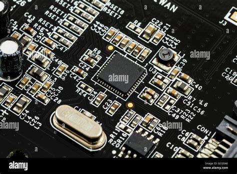
Integrated circuit (IC) Printed Circuit Boards (PCBs) are the most advanced and complex types of PCBs used in the electronics industry today. These high-density, high-performance PCBs are designed to package and interconnect semiconductor chips or dies, enabling the creation of cutting-edge electronic devices and systems.
IC PCBs can be broadly categorized into two main types: IC substrates and IC probe cards. Both play crucial roles in the manufacturing and testing of semiconductor devices, but they serve different purposes and have distinct characteristics.
In this article, we will delve into the world of IC substrates and IC probe cards, exploring their definitions, applications, manufacturing processes, and the latest advancements in these fields.
What is an IC Substrate?
An IC substrate, also known as a chip carrier or package substrate, is a specialized PCB that serves as an interconnect between a semiconductor chip (die) and the main PCB or motherboard of an electronic device. The primary function of an IC substrate is to provide electrical connections, mechanical support, and thermal management for the chip.
Key Features of IC Substrates
- High-density interconnects: IC substrates feature fine-pitch traces and vias to accommodate the high pin count and small pitch of modern semiconductor chips.
- Multi-layer structure: To achieve high interconnect density, IC substrates often consist of multiple layers of conductive traces and dielectric materials.
- Thermal management: IC substrates incorporate Thermal Vias and heat spreaders to dissipate heat generated by the chip efficiently.
- Mechanical support: The substrate provides a stable and robust platform for the chip, protecting it from physical damage and environmental factors.
Applications of IC Substrates
IC substrates are used in a wide range of electronic devices and applications, including:
- Smartphones and tablets
- Computers and laptops
- Data centers and servers
- Automotive electronics
- Industrial automation and control systems
- Medical devices and equipment
- Aerospace and defense systems

Manufacturing Process of IC Substrates
The manufacturing process of IC substrates involves several complex steps and advanced technologies. Here is an overview of the key stages:
- Material selection: The base material for IC substrates is typically a glass-reinforced epoxy laminate, such as FR-4 or BT (Bismaleimide Triazine).
- Patterning: The conductive traces and vias are patterned onto the substrate using photolithography and etching processes.
- Lamination: Multiple layers of patterned substrates are laminated together using heat and pressure to form a multi-layer structure.
- Drilling and plating: Through-holes and micro-vias are drilled and plated with conductive materials to establish inter-layer connections.
- Surface finishing: The exposed copper traces are coated with protective and solderable surface finishes, such as ENIG (Electroless Nickel Immersion Gold) or OSP (Organic Solderability Preservative).
- Inspection and testing: The finished IC substrates undergo rigorous inspection and testing to ensure quality and reliability.
Advancements in IC Substrate Manufacturing
The demand for higher performance, smaller form factors, and increased functionality in electronic devices has driven several advancements in IC substrate manufacturing:
- Finer pitch and higher density: IC substrates now feature trace widths and spacings as small as 15-20 microns, enabling higher interconnect density.
- Advanced materials: New substrate materials, such as polyimide and low-loss dielectrics, are being developed to improve electrical performance and thermal management.
- Embedded components: Passive components, such as capacitors and resistors, can be embedded within the substrate layers to save space and enhance performance.
- 3D packaging: 3D IC packaging technologies, such as through-silicon vias (TSVs) and stacked dies, are being integrated with IC substrates to create highly compact and efficient packages.

What is an IC Probe Card?
An IC probe card is a specialized PCB used in the testing of semiconductor wafers before they are diced into individual chips. The probe card serves as an interface between the wafer and the automatic test equipment (ATE), enabling the electrical characterization and Functional Testing of the integrated circuits on the wafer.
Key Features of IC Probe Cards
- Probe tips: IC probe cards are equipped with an array of fine-pitch probe tips that make contact with the bond pads or bumps on the wafer.
- High pin count: Modern probe cards can have thousands of probe tips to test high-density wafers with numerous devices.
- Precision alignment: The probe tips must be precisely aligned with the wafer’s contact points to ensure accurate and reliable testing.
- Mechanical compliance: Probe cards incorporate spring-like structures or elastomeric materials to compensate for minor variations in wafer topology and ensure consistent contact.
Applications of IC Probe Cards
IC probe cards are essential tools in the semiconductor manufacturing process, used for various testing applications:
- Wafer sort: Probe cards are used to perform electrical tests on individual dies while still on the wafer, identifying defective or sub-par devices before packaging.
- Burn-in testing: Some probe cards are designed for extended testing under elevated temperatures and voltages to screen out early failures.
- Parametric testing: Probe cards enable the measurement of key electrical parameters, such as voltage, current, and capacitance, to verify device performance.
- Functional testing: Probe cards can be used to perform basic functional tests on the devices, ensuring they meet the desired specifications.

Manufacturing Process of IC Probe Cards
The manufacturing process of IC probe cards involves several specialized steps and technologies:
- Substrate fabrication: The probe card substrate is typically made of a high-performance PCB material, such as polyimide or ceramic, to ensure stability and thermal compatibility.
- Probe tip fabrication: The probe tips are usually made of tungsten, beryllium-copper, or palladium alloys, and are fabricated using precision machining or micro-electro-mechanical systems (MEMS) technologies.
- Probe tip attachment: The probe tips are attached to the substrate using advanced bonding techniques, such as wire bonding, soldering, or conductive adhesives.
- Planarization: The probe tips are mechanically planarized to ensure uniform contact with the wafer surface.
- Assembly and calibration: The probe card is assembled with the necessary electrical components and calibrated to meet the specific testing requirements.
Advancements in IC Probe Card Technology
As semiconductor devices continue to shrink in size and increase in complexity, IC probe card technology has evolved to keep pace:
- MEMS probe tips: MEMS-based probe tips offer higher density, finer pitch, and improved mechanical compliance compared to traditional probe tips.
- Active probe cards: Active probe cards incorporate active electronic components, such as amplifiers and switches, to enhance signal integrity and reduce test time.
- Multi-DUT testing: Advanced probe cards can simultaneously test multiple devices on the wafer, significantly increasing throughput and reducing costs.
- Adaptive probe cards: Probe cards with adaptive control mechanisms can dynamically adjust the probe tip positions to compensate for wafer warpage or variations in contact resistance.
FAQ
-
Q: What is the difference between an IC substrate and an IC probe card?
A: An IC substrate is a PCB that packages and interconnects a semiconductor chip, while an IC probe card is a specialized PCB used for testing semiconductor wafers before they are diced into individual chips. -
Q: Why are IC substrates important in electronic devices?
A: IC substrates provide electrical connections, mechanical support, and thermal management for semiconductor chips, enabling the creation of compact, high-performance electronic devices. -
Q: What are the key challenges in manufacturing IC substrates?
A: The main challenges in IC substrate manufacturing include achieving high interconnect density, managing thermal dissipation, ensuring mechanical stability, and integrating advanced packaging technologies. -
Q: How do IC probe cards contribute to the semiconductor manufacturing process?
A: IC probe cards are essential for testing semiconductor wafers before packaging, enabling the identification of defective devices, measurement of electrical parameters, and verification of functional performance. -
Q: What are some of the latest advancements in IC probe card technology?
A: Recent advancements in IC probe card technology include the use of MEMS probe tips, active electronic components, multi-DUT testing capabilities, and adaptive control mechanisms for improved accuracy and throughput.
Conclusion
IC substrates and IC probe cards are two of the most advanced and critical types of PCBs in the electronics industry. IC substrates play a vital role in packaging and interconnecting semiconductor chips, while IC probe cards are essential for testing wafers before dicing.
As the demand for smaller, faster, and more complex electronic devices continues to grow, innovations in IC substrate and probe card technologies will be crucial to meeting these challenges. From advanced materials and packaging techniques to MEMS probe tips and adaptive control mechanisms, the future of IC PCBs is filled with exciting possibilities.
By understanding the fundamentals, applications, and latest advancements in IC substrates and probe cards, engineers, designers, and manufacturers can stay at the forefront of this rapidly evolving field and create the next generation of cutting-edge electronic devices.


Leave a Reply