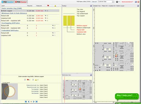
What is PCB Visualizer?
PCB Visualizer is a powerful software tool that allows electronics engineers and PCB designers to visually inspect and analyze printed circuit board designs in 3D. It provides an intuitive and interactive way to explore the physical layout, components, and connections of a PCB before it goes into production.
Key Features of PCB Visualizer
| Feature | Description |
|---|---|
| 3D Visualization | Renders a realistic 3D model of the PCB, allowing you to view it from any angle |
| Component Placement | Shows the exact location and orientation of each component on the board |
| Trace Routing | Displays the copper traces that connect components, including vias and layers |
| Design Rule Checking | Verifies the PCB design against a set of predefined rules to catch errors early |
| Collaboration | Enables team members to view, comment on, and discuss the PCB design in real-time |
Why is PCB Visualization Important?
Visualizing a PCB design is crucial for several reasons:
-
Catching Design Errors Early: By visually inspecting the PCB layout in 3D, designers can identify potential issues such as component collisions, incorrect orientations, or violated clearances before the board is sent for manufacturing. This saves time and money by avoiding costly rework or redesigns.
-
Enhancing Communication: PCB Visualizer enables clear communication among team members, including engineers, designers, and manufacturers. It provides a common visual language that everyone can understand, reducing misinterpretations and improving collaboration.
-
Optimizing Component Placement: With a 3D view of the PCB, designers can experiment with different component placements to optimize space utilization, thermal management, and signal integrity. They can easily move components around and see the impact on the overall layout.
-
Verifying Manufacturability: PCB Visualizer helps ensure that the design is manufacturable by checking it against design rules and constraints. It can highlight issues such as insufficient clearances, improper trace widths, or missing solder mask openings, allowing designers to make necessary adjustments.

How PCB Visualizer Enhances the Design Workflow
Incorporating PCB Visualizer into the electronics design workflow brings several benefits:
1. Iterative Design Process
With PCB Visualizer, designers can quickly iterate on their designs by making changes and seeing the results in real-time. They can experiment with different component placements, trace routing strategies, and layer stackups to find the optimal solution. This iterative approach leads to better designs in less time.
2. Collaborative Design Reviews
PCB Visualizer enables remote design reviews and collaboration. Team members can access the 3D model of the PCB from anywhere and provide feedback or suggestions. They can leave comments, mark areas of concern, and discuss design choices directly within the visualization environment. This collaborative approach ensures that everyone is on the same page and reduces the chances of miscommunication.
3. Integration with Other Tools
Many PCB Visualizer tools integrate seamlessly with other electronics design software, such as schematic capture and PCB layout tools. This integration allows designers to import their designs directly into the visualizer, maintaining the integrity of the data. Any changes made in the original design tools are automatically reflected in the 3D visualization, ensuring consistency throughout the design process.

Real-World Applications of PCB Visualizer
PCB Visualizer finds applications across various industries and projects:
1. Consumer Electronics
In the fast-paced world of consumer electronics, time-to-market is critical. PCB Visualizer helps designers quickly prototype and iterate on their designs, ensuring that products are ready for mass production in the shortest possible time. It allows designers to visualize how components fit together, optimize layouts for manufacturability, and catch any potential issues early in the design phase.
2. Automotive Electronics
Modern vehicles rely heavily on electronic systems for various functions, from infotainment to advanced driver assistance systems (ADAS). PCB Visualizer is essential for designing reliable and compact electronic modules that can withstand the harsh automotive environment. It helps designers ensure proper component placement, thermal management, and signal integrity in these safety-critical systems.
3. Medical Devices
Medical devices require the highest level of reliability and precision. PCB Visualizer enables designers to create compact and highly integrated electronic assemblies for medical applications. It helps ensure that the PCB layout meets the stringent requirements for signal integrity, EMI/EMC compliance, and manufacturability. By visually inspecting the design in 3D, designers can identify potential issues and make necessary adjustments to meet the strict regulatory standards.
4. Aerospace and Defense
In the aerospace and defense industry, electronic systems must operate reliably in extreme conditions, such as high altitudes, extreme temperatures, and high levels of vibration. PCB Visualizer helps designers create robust and resilient PCB layouts that can withstand these challenges. It allows designers to optimize component placement, ensure proper grounding and shielding, and verify the mechanical integrity of the assembly.

Case Studies
1. Smartphone Manufacturer
A leading smartphone manufacturer used PCB Visualizer to optimize the layout of their latest flagship device. By visually exploring the 3D model of the PCB, they were able to identify areas where components could be rearranged to minimize the overall board size and improve signal integrity. The visualizer also helped them ensure proper clearances and avoid any potential collisions between components. As a result, they were able to create a more compact and efficient design, which translated into better performance and longer battery life for the end-user.
2. Automotive Supplier
An automotive supplier used PCB Visualizer to design a complex electronic control unit (ECU) for a new vehicle platform. The ECU had to integrate multiple functions, including engine control, transmission control, and body electronics. PCB Visualizer allowed the design team to collaborate remotely and iterate on the layout quickly. They were able to optimize the placement of high-speed components, ensure proper grounding and shielding, and verify the manufacturability of the design. The visualizer’s design rule checking feature caught several potential issues early in the design process, saving the company significant time and cost in redesigns.
Frequently Asked Questions (FAQ)
1. Is PCB Visualizer only for complex designs, or can it be used for simple PCBs as well?
PCB Visualizer is valuable for PCB designs of all complexities. While it is particularly beneficial for complex, high-density designs with multiple layers and numerous components, it can also be used for simpler PCBs. Even in simple designs, PCB Visualizer helps ensure proper component placement, trace routing, and manufacturability.
2. Can PCB Visualizer be used by individuals, or is it only for teams?
PCB Visualizer is suitable for both individual designers and teams. Individuals can use it to visually inspect and optimize their designs, while teams can leverage its collaboration features for remote design reviews and discussions. It facilitates communication and ensures that everyone has a clear understanding of the PCB layout.
3. Does PCB Visualizer require specialized hardware or high-end computing resources?
Most PCB Visualizer tools are designed to run on standard computer hardware and do not require specialized or high-end resources. However, for very large and complex designs with numerous components and layers, a more powerful computer with a dedicated graphics card may provide better performance and faster rendering speeds.
4. How does PCB Visualizer handle different layer stackups and materials?
PCB Visualizer tools typically allow designers to define the layer stackup and specify the materials used for each layer. This includes the substrate material, copper thickness, and dielectric properties. The visualizer takes this information into account when rendering the 3D model and performing design rule checks. It ensures that the visualization accurately represents the physical characteristics of the PCB.
5. Can PCB Visualizer export the 3D model for use in other software or for 3D printing?
Yes, most PCB Visualizer tools offer the capability to export the 3D model of the PCB in various file formats, such as STEP, IGES, or OBJ. These exported files can be used in other software applications, such as mechanical CAD tools, for further analysis or integration with enclosure designs. Additionally, the exported models can be 3D printed to create physical prototypes of the PCB Assembly.
Conclusion
PCB Visualizer is a game-changer in the world of electronics design. It provides designers with a powerful tool to visually inspect, analyze, and optimize their PCB layouts in 3D. By catching design errors early, enhancing communication, and facilitating collaboration, PCB Visualizer streamlines the design process and ensures the creation of high-quality, manufacturable PCBs.
Whether you are working on consumer electronics, automotive systems, medical devices, or aerospace and defense projects, PCB Visualizer is an essential tool in your design toolkit. It enables you to create compact, reliable, and efficient electronic assemblies that meet the specific requirements of your industry.
As PCB designs continue to become more complex and demanding, the role of PCB Visualizer will only grow in importance. By embracing this technology and incorporating it into your design workflow, you can stay ahead of the curve and deliver innovative, high-performance electronic products to market faster than ever before.


Leave a Reply