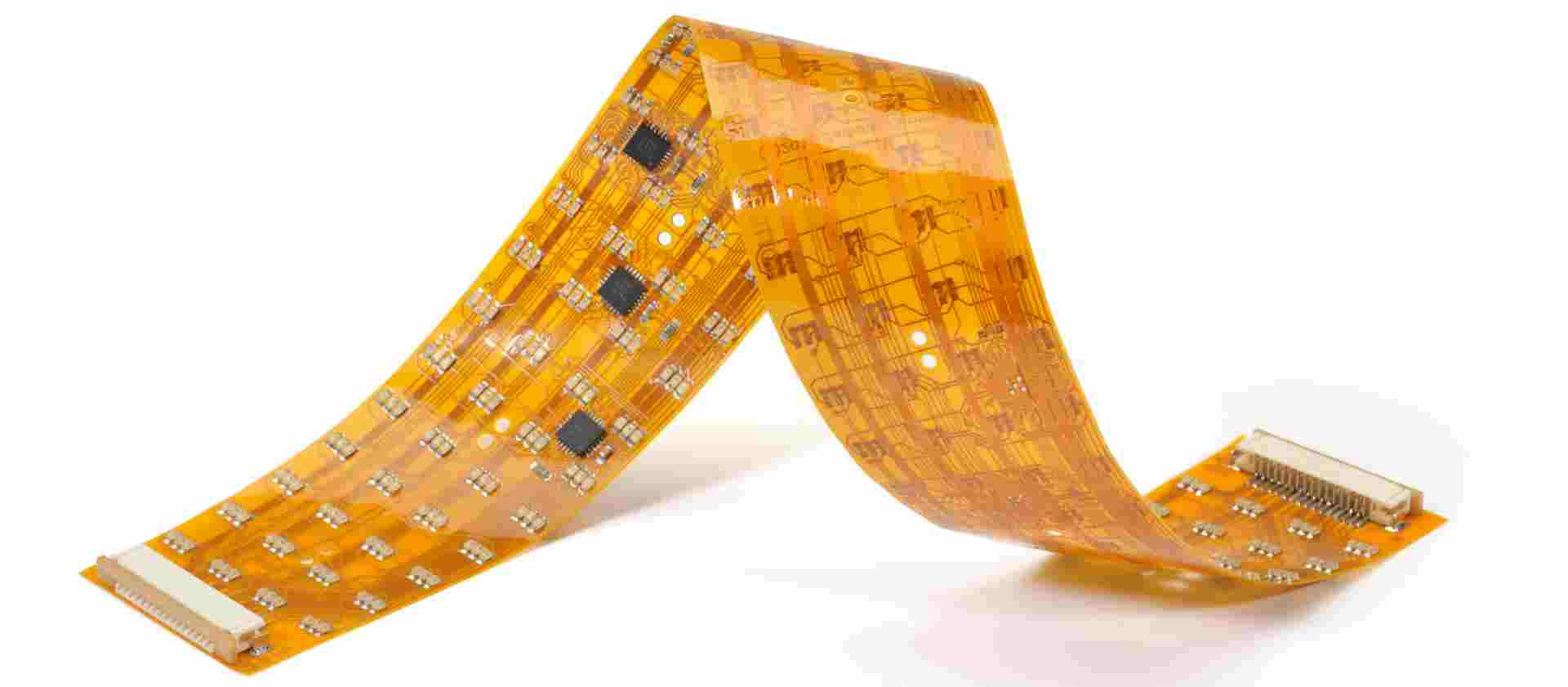
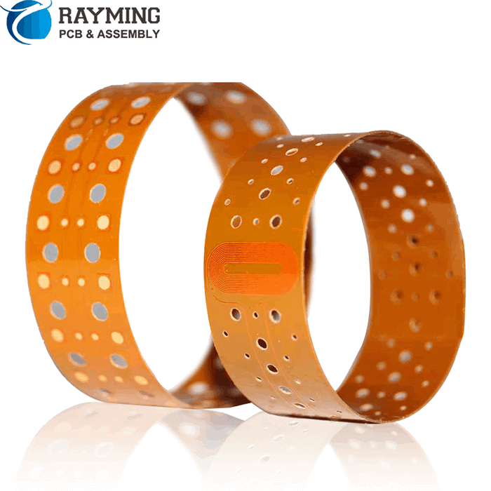
Flexible printed circuit boards (flex PCBs or flex circuits) are a type of printed circuit board that can bend and flex. They are made with flexible substrate materials like polyimide or polyester instead of traditional rigid materials like FR-4. Flex PCBs are useful for applications where the circuit needs to move or adapt to different shapes.
One important specification for designing and using flex PCBs is the minimum bend radius. The bend radius defines how tight of a bend the flex PCB can make without damaging the circuitry. Understanding the factors that affect bend radius is key to creating robust and reliable flex PCB designs.
What is Bend Radius?
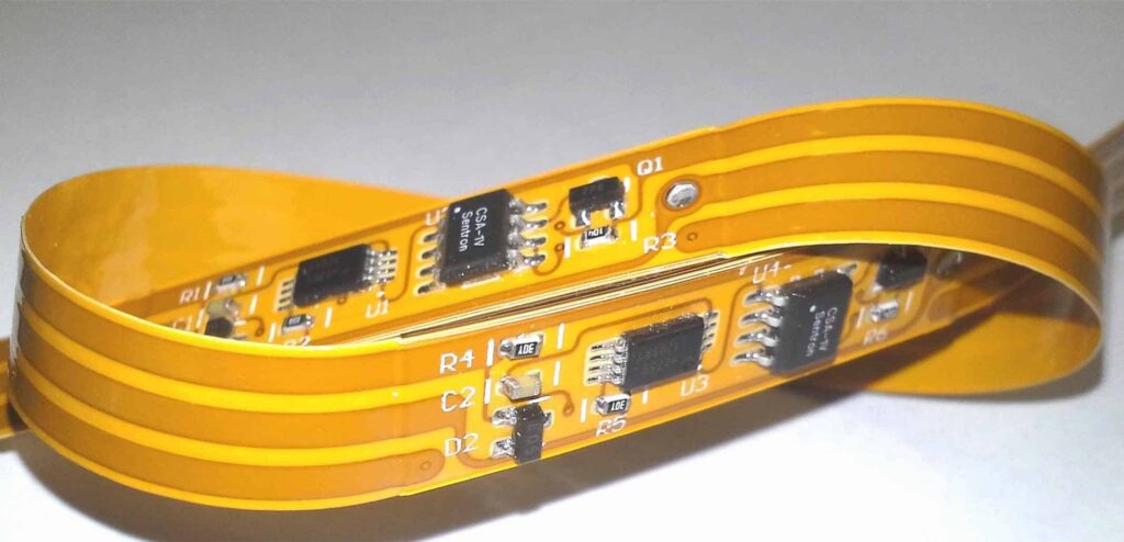
The bend radius of a flex PCB refers to the minimum inside radius that the flex circuit can be bent without causing damage. It is typically represented by the variable R.
The bend radius is measured to the inside curved edge of the flex PCB, as shown in the diagram. A smaller bend radius allows for tighter folds and bends. The actual bend radius depends on factors like:
- Flex PCB layer stackup
- Conductor width and spacing
- Flexible substrate material used
- Coverlay and stiffener materials
- Expected number of bend cycles
The minimum bend radius is an important guideline for both design and use. Bending below this radius can crack substrates, delaminate layers, break conductors, and damage components. Excessively tight folds create fatigue and will reduce the lifetime of a flex PCB.
Factors That Affect Bend Radius
Several variables will determine the minimum bend radius that can be tolerated by a flex PCB without failure.
1. Substrate Material
The flexible substrate is the base material that the conductors are laminated onto. Polyimide films like Kapton are most commonly used. Others include polyester (PET), polyethylene (PE), and fluoropolymers (PTFE). The minimum bend radius correlates closely with the flexural modulus of the substrate. Materials with higher flexural modulus (stiffer) have larger minimum bend radii. Polyimide can be formulated in different thicknesses and grades with different moduli to tune the bend radius. Thinner polyimide allows for tighter bends.
2. Conductor Width and Spacing
The width and spacing of conductors is a major factor in bend radius. A primary failure mode is cracking of the copper traces during bending stresses. Wider conductors with larger spacing can tolerate tighter bends. Common flex PCB conductors are 12-25 μm thick rolled annealed copper foil. Guidelines suggest the minimum bend radius should be at least 10 times the conductor thickness. For 12 μm conductors, the minimum radius would be approximately 120 μm. Wider spacing further prevents cracks from propagating between lines.
3. Number of Layers
Flex circuits can be fabricated with multiple conductive layers laminated together. Additional layers will increase the overall thickness and stiffness. More layers require larger bend radii to prevent damage. Two-layer flex designs can have bend radii around 75-125% of the substrate’s minimum, while high layer counts (>6) may require 2-3 times the substrate minimum.
4. Coverlay
Coverlay is a protective insulating layer laminated over the conductor pattern for insulation and mechanical support. The thickness and modulus of coverlay impacts the bend radius. Softer, thinner coverlay allows for tighter folds. No coverlay permits the smallest radius, but leaves conductors exposed.
5. Stiffeners
Discrete stiffeners are sometimes added to flex PCBs to offer localized reinforcement and guard against overbending. Common materials are polyimide, PTFE, or acrylic. Stiffeners will locally increase the bend radius. Their placement should be considered early when calculating the overall minimum bend radius.
6. Expected Cycles
The number of bend cycles a flex PCB will experience over its lifetime influences the acceptable minimum radius. More extreme bending leads to fatigue and material stress. Lower radii can be used for applications with infrequent bends, while dynamic flexing requires more conservative margins to prevent conductor cracks from propagating.
By considering all these factors, designers can predict and verify the minimum bend radius for a flex PCB layer stackup and conductor layout.
Typical Bend Radii
Typical minimum bend radii for common flex PCB materials are:
| Flex PCB Type | Typical Minimum Bend Radius |
|---|---|
| Polyimide, single-layer | 1-2 x substrate thickness |
| Polyimide, multilayer | 3-5 x substrate thickness |
| Polyester, PET | 10-20 x substrate thickness |
| Polyimide, Kapton | 5-10 x substrate thickness |
For example, a 25 μm thick Kapton substrate may have a minimum bend radius of 125-250 μm (.125-.25 mm). Polyester films have larger bend radii than polyimide.
More specific minimum bend radii take into account conductor spacing, layer count, and other constraints mentioned earlier. Manufacturers can provide radius recommendations based on the design. IPC standards suggest a minimum 10X conductor thickness rule.
Bend Radius Testing
Bend radius specifications should be validated through testing. Sample PCBs can be bent over mandrels with descending radii until failures like cracked traces occur. This verifies the minimum radius. Samples should also be fatigue tested by repeatedly bending around the minimum radius. Testing can refine the bend radius guidelines and account for production variability between PCB suppliers.
Common test methods include:
- Mandrel wrap test: Wrapping PCB sample around mandrels with decreasing diameters until failure.
- Wedge test: Bending PCB sample down onto wedge tips of decreasing radii until failure.
- Roller bend test: Bending PCB through rollers of decreasing diameters. Checks ability to resist dynamic/cyclic bending.
- Flexural modulus testing: Characterizing modulus and yield strength of materials. Used to derive theoretical minimum bend radii.
Design Rules for Bend Radius
Here are some key guidelines designers should follow to avoid bend radius issues:
- Determine expected use conditions – How will the flex PCB bend and flex in the application? Define required bend radii.
- Use generous conductor widths and spacing – Larger features tolerate tighter bends. Aim for at least 10X conductor thickness.
- Orient conductors along the bend axis – Conductors oriented parallel to the bend axis see less strain than perpendicular ones.
- Avoid 90° bends – Gradual bends distribute strain over larger area. Sharp 90° bends concentrate stress.
- Watch component placement near folds – Don’t place fragile components near a fold line. Plan ahead for tight radii.
- Leave slits/cutouts along bend lines – Removing material along bend axes allows sharper localized bends.
- Use generous bend radius assumptions – Leave margin and assume worst-case conditions. Optimize after prototyping.
Following these guidelines and communicating expected bend radii to your PCB manufacturer will prevent failures and ensure reliable flex PCB performance.
Effect of Tight Bend Radii
Bending flex PCBs below the minimum bend radius has several negative effects:
Conductor cracks – Excessive tensile strain perpendicular to conductor axes cracks and ruptures the copper traces. The PCB loses electrical connectivity.
Substrate cracks – Polyimide and other substrate materials can crack under the bend strain, damaging the base insulating layers.
Delamination – Layers can detach and separate from each other at fold lines when subjected to repeated dynamic bending.
Broken components – Brittle components like resistors, capacitors, and chips fracture under bending stresses if placed near fold lines.
Flexural fatigue – Repeated cyclical bending below the minimum radius weakens materials and interconnections over time. Failures occur after repeated folds.
Warping – Residual stresses from tight folds can warp the PCB shape over time and cause registration issues during assembly.
Cracked solder joints – Solder connections to components fail from cyclic fatigue when bent repeatedly below the minimum radius.
Traces separating from pads – The bond between traces and component pads weakens and detaches after repeated extreme bending.
Tenting of plated through holes – Mechanical deformation around plated through holes can cause cracks in the copper plating inside.
These damage mechanisms demonstrate why adhering closely to the specified minimum bend radius of your flex PCB is critical. Thorough engineering and testing is required to define realistic guidelines. Margin should be designed in for variability. Excessively tight folds will eventually cause circuit failures.
FQA
What are the main factors that determine the minimum bend radius of a flex PCB?
The minimum bend radius depends on the substrate material, conductor thickness and spacing, number of conductive layers, use of coverlay, placement of stiffeners, and expected number of bend cycles. Thinner flex circuits with fewer layers, wider traces, and dynamic applications require larger minimum bend radii.
Why is bend radius important for flex PCB reliability?
Bending flex PCBs below the minimum radius can crack substrates, delaminate layers, rupture traces, and fracture components. Tight folds create stresses that impact performance and shorten the product lifetime. Adequate bend radius prevents premature failures.
How can you design a flex PCB for tighter bend radii?
Strategies to enable tighter folds include using thin substrate, fewer layers, wider conductor spacing, removing material along folds, and avoiding brittle components near bends. Gradual bends are better than sharp 90° angles. Always have margin between design and minimum bend radius.
How do I determine the minimum bend radius for a new flex PCB design?
Work with your flex PCB manufacturer to understand the minimum bend radius based on materials used, layer stackup, trace spacing, and other design factors. Validate through testing of prototypes. Leave margin in initial designs and optimize the radius with field testing.
What problems occur when a flex PCB is bent below its minimum radius?
Bending too tight can crack substrates, delaminate layers, break traces, fatigue materials, warp the PCB, and break solder joints. It accelerates failure mechanisms and reduces the operating lifetime. Tight folds risk immediate or eventual circuit failure.


Leave a Reply