Table of Contents
- What is Solder mask?
- Composition of Solder Mask
- Types of Solder Mask
- Solder Mask Application Methods
- Functions of Solder Mask
- Solder Mask Colors
- Solder Mask Design Considerations
- Frequently Asked Questions (FAQ)
- Conclusion
What is Solder Mask?
Solder mask is a thin, protective coating applied to the copper traces of a printed circuit board (PCB) during the manufacturing process. It is typically a polymer-based material that is applied as a liquid and then cured through exposure to UV light or heat. The primary purpose of solder mask is to insulate and protect the copper traces from oxidation, contaminants, and physical damage while also preventing solder bridges from forming between closely spaced pads during the soldering process.
Solder mask is usually applied over the entire PCB surface, except for areas where components will be soldered, such as pads, through-holes, and vias. These exposed areas are left uncovered to allow for proper electrical connections during the assembly process.

Composition of Solder Mask
Modern solder masks are typically composed of a combination of epoxy resins, hardeners, fillers, and pigments. The exact composition may vary depending on the specific requirements of the PCB and the manufacturer’s proprietary formulations. The key components of solder mask include:
-
Epoxy resins: These resins form the base of the solder mask and provide excellent insulation properties, chemical resistance, and adhesion to the copper surface.
-
Hardeners: Hardeners are added to the epoxy resins to initiate the curing process and improve the mechanical properties of the solder mask, such as toughness and durability.
-
Fillers: Fillers, such as silica or alumina, are used to enhance the thermal and mechanical properties of the solder mask, as well as to control its viscosity and flow characteristics during application.
-
Pigments: Pigments are added to the solder mask to provide color and improve its opacity. The most common solder mask colors are green, blue, red, and black, although custom colors can be formulated upon request.

Types of Solder Mask
There are two main types of solder mask used in PCB manufacturing:
-
Liquid Photoimageable Solder Mask (LPSM): LPSM is the most common type of solder mask used in the industry. It is applied as a liquid coating and then exposed to UV light through a photomask, which selectively hardens the exposed areas. The unexposed areas are then removed during the development process, leaving the desired solder mask pattern on the PCB.
-
Dry Film Solder Mask (DFSM): DFSM is a solid film that is laminated onto the PCB surface using heat and pressure. The film is then exposed to UV light through a photomask, and the unexposed areas are removed during the development process, similar to LPSM. DFSM is less commonly used than LPSM due to its higher cost and lower resolution capabilities.

Solder Mask Application Methods
The application of solder mask involves several steps to ensure proper coverage, thickness, and accuracy. The most common solder mask application methods include:
-
Screen Printing: In this method, a thin stainless steel mesh with a patterned emulsion is used to selectively apply the liquid solder mask onto the PCB surface. The screen is placed over the PCB, and the solder mask is forced through the open areas of the mesh using a squeegee. This method is suitable for low-volume production and larger feature sizes.
-
Curtain Coating: Curtain coating involves continuously passing the PCB through a falling curtain of liquid solder mask. This method ensures a uniform coating thickness across the entire board and is suitable for high-volume production. However, it requires additional steps to remove the solder mask from areas where it is not desired, such as pads and through-holes.
-
Spray Coating: In spray coating, the liquid solder mask is atomized and sprayed onto the PCB surface using a spray nozzle. This method provides good coverage and can accommodate complex PCB geometries. However, it may result in a less uniform coating thickness compared to other methods.
After the solder mask is applied, it undergoes a curing process, which typically involves exposure to UV light or heat to cross-link the polymer chains and harden the material. The cured solder mask provides a durable, protective layer that can withstand the rigors of the soldering process and the operating environment of the final electronic device.
Functions of Solder Mask
Solder mask serves several critical functions in PCB manufacturing and assembly:
-
Insulation: Solder mask acts as an insulating layer between the copper traces and the environment, preventing short circuits and electrical leakage.
-
Protection against oxidation: Exposed copper traces can quickly oxidize when exposed to air, leading to decreased solderability and poor electrical connections. Solder mask protects the copper from oxidation, ensuring reliable soldering and long-term stability.
-
Solder bridge prevention: During the soldering process, molten solder can inadvertently bridge adjacent pads, creating short circuits. Solder mask helps prevent these bridges by covering the spaces between pads and acting as a barrier to the flow of solder.
-
Improved aesthetics: Solder mask provides a uniform, professional appearance to the PCB, enhancing its visual appeal and making it easier to identify components and traces.
-
Increased durability: Solder mask protects the PCB from physical damage, such as scratches and abrasions, as well as from environmental factors like moisture, dust, and chemicals.
Solder Mask Colors
While the most common solder mask color is green, various colors are available to suit different applications and design preferences. Some of the most popular solder mask colors include:
| Color | Pantone Code | Typical Uses |
|---|---|---|
| Green | Pantone 340C | General-purpose, industrial, and consumer electronics |
| Blue | Pantone 294C | High-end consumer electronics, aerospace, and military applications |
| Red | Pantone 185C | Automotive, medical devices, and high-reliability applications |
| Black | Pantone Black C | High-end audio equipment, luxury consumer electronics, and stealth applications |
| White | Pantone White C | LED lighting, reflective surfaces, and high-contrast designs |
| Yellow | Pantone 124C | Warning labels, safety-critical applications, and high-visibility designs |
The choice of solder mask color is often dictated by the specific application, industry standards, and aesthetic preferences. Some industries, such as aerospace and military, may have specific color requirements for PCBs to ensure consistency and compliance with regulations.
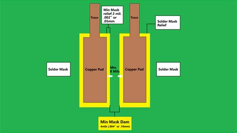
Solder Mask Design Considerations
When designing a PCB, several factors must be considered to ensure the proper application and performance of the solder mask:
-
Solder mask clearance: The space between the edge of a pad and the solder mask, known as the solder mask clearance, must be carefully designed to allow for proper solder wetting and to accommodate any potential misalignment during the solder mask application process. Typical solder mask clearances range from 0.05mm to 0.1mm, depending on the PCB’s feature size and manufacturing capabilities.
-
Solder mask expansion: During the curing process, solder mask may expand slightly, which can cause it to encroach onto pads and other exposed areas. To compensate for this expansion, designers must include additional clearance around pads and other critical features.
-
Solder mask thickness: The thickness of the solder mask can impact its insulation properties, durability, and the ability to properly apply and cure the material. Typical solder mask thicknesses range from 0.01mm to 0.03mm, with thicker coatings providing better insulation and protection but potentially impacting the PCB’s dimensional tolerances.
-
Solder mask color and opacity: The choice of solder mask color and its opacity can affect the PCB’s aesthetics, legibility of markings, and the performance of optical components, such as LEDs or photosensors. Designers must consider the specific requirements of the application when selecting the solder mask color and ensuring that it provides sufficient opacity to protect the underlying copper traces.
-
Solder mask compatibility: The solder mask material must be compatible with the PCB Substrate, copper traces, and the soldering process to ensure proper adhesion, durability, and performance. Designers should work closely with their PCB manufacturer to select the appropriate solder mask material for their specific application.
By carefully considering these design factors and working with experienced PCB manufacturers, designers can ensure that the solder mask performs its intended functions and contributes to the overall reliability and longevity of the electronic device.
Frequently Asked Questions (FAQ)
-
Q: What is the difference between solder mask and conformal coating?
A: Solder mask is applied during the PCB manufacturing process and is primarily used to protect the copper traces from oxidation and prevent solder bridges. Conformal coating, on the other hand, is applied after the PCB Assembly process and provides additional protection against moisture, dust, and other environmental factors. -
Q: Can solder mask be removed for rework or repair?
A: Yes, solder mask can be selectively removed using abrasive methods, such as sanding or scraping, or chemical methods, such as using solder mask strippers. However, removing solder mask can be challenging and may damage the underlying copper traces if not done carefully. -
Q: Are there any disadvantages to using solder mask on a PCB?
A: While solder mask provides numerous benefits, it can slightly increase the PCB’s manufacturing cost and lead time. Additionally, if not applied properly, solder mask can cause issues such as poor adhesion, uneven coverage, or bubbles, which may impact the PCB’s performance and reliability. -
Q: Can solder mask be applied to Flexible PCBs?
A: Yes, specialized solder mask materials, known as flexible solder masks, are available for use on flexible PCBs. These materials are formulated to withstand the bending and flexing that flexible PCBs undergo during use, while still providing the necessary insulation and protection. -
Q: How does solder mask affect the impedance of PCB Traces?
A: Solder mask can slightly affect the impedance of PCB traces by altering the dielectric constant of the material surrounding the traces. However, this effect is generally minimal and can be accounted for during the PCB design process by adjusting the trace width and spacing to achieve the desired impedance.
Conclusion
Solder mask is a critical component in PCB manufacturing, providing essential insulation, protection, and aesthetic benefits to electronic devices. By understanding the composition, types, application methods, and design considerations associated with solder mask, engineers and designers can make informed decisions when developing PCBs for various applications.
As PCB technologies continue to advance, with smaller feature sizes, higher component densities, and more demanding performance requirements, the role of solder mask in ensuring the reliability and longevity of electronic devices will only become more crucial. By staying up-to-date with the latest solder mask materials, processes, and design techniques, the electronics industry can continue to push the boundaries of innovation and create ever-more advanced and reliable products.


Leave a Reply