Introduction to Solder Mask
Solder mask, also known as solder resist or solder stop, is a thin protective layer applied to the copper traces of a printed circuit board (PCB). This coating serves multiple purposes, including preventing solder bridges from forming between closely spaced solder pads, protecting the copper from oxidation, and providing a more aesthetically pleasing appearance to the PCB. Solder mask is a crucial component in the manufacturing process of PCBs, as it ensures the proper functioning and reliability of the final product.
What is Solder Mask Made Of?
Solder mask is typically made of a polymer-based ink that is applied to the PCB surface. The most common types of solder mask materials are:
-
Liquid Photoimageable Solder Mask (LPSM): This type of solder mask is applied as a liquid and then exposed to UV light to cure and harden. LPSM offers excellent resolution and is suitable for fine-pitch components.
-
Dry Film Photoimageable Solder Mask (DFSM): DFSM is applied as a dry film and then exposed to UV light to cure. It provides good coverage and is often used for larger components and connectors.
-
Epoxy Liquid Solder Mask: This type of solder mask is a two-part epoxy that is mixed and applied to the PCB surface. It offers excellent chemical resistance and durability.
Properties of Solder Mask
A high-quality solder mask should possess the following properties:
- Good adhesion to the copper surface
- High resistance to solvents and chemicals
- Excellent dielectric properties to prevent short circuits
- Thermal stability to withstand Soldering Temperatures
- Smooth surface finish for improved aesthetics and component placement
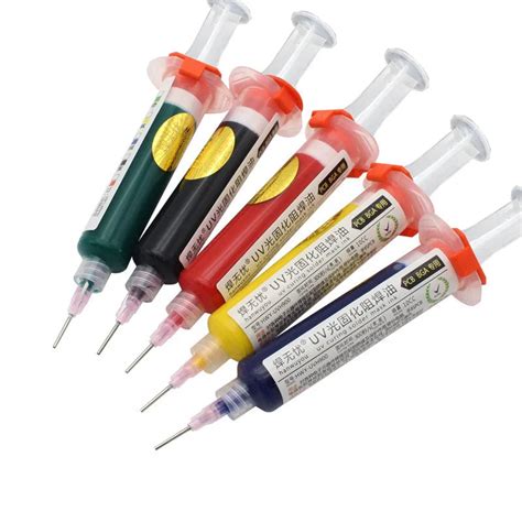
Colors of Solder Mask
Solder mask is available in a variety of colors, with green being the most common. Other popular colors include:
- Blue
- Red
- Yellow
- Black
- White
The choice of color is often based on aesthetics, but it can also serve a functional purpose. For example, white solder mask is sometimes used for LED lighting applications to improve light reflectivity.
Solder Mask Application Process
The application of solder mask involves several steps to ensure proper coverage and adhesion to the PCB surface.
Surface Preparation
Before applying the solder mask, the PCB surface must be thoroughly cleaned to remove any contaminants, such as dirt, grease, or oxidation. This is typically done using a combination of chemical and mechanical cleaning methods.
Solder Mask Application
The solder mask is then applied to the PCB surface using one of the following methods:
-
Screen Printing: A stencil is used to apply the solder mask ink to the desired areas of the PCB. This method is suitable for larger components and connectors.
-
Spraying: The solder mask is sprayed onto the PCB surface using a spray gun. This method provides a more even coverage and is suitable for finer details.
-
Curtain Coating: The PCB is passed through a curtain of solder mask ink, which coats the entire surface. Excess ink is then removed using a squeegee or air knife.
Curing
After application, the solder mask must be cured to harden and adhere to the PCB surface. This is typically done using UV light or heat, depending on the type of solder mask material used.
Inspection and Touch-Up
Once the solder mask has been cured, the PCB is inspected for any defects or areas of incomplete coverage. Any necessary touch-ups are made using a small brush or pen applicator.

Solder Mask Design Considerations
When designing a PCB, there are several factors to consider related to solder mask:
Solder Mask Clearance
Solder mask clearance refers to the distance between the edge of a solder pad and the opening in the solder mask. This clearance is necessary to ensure proper soldering and prevent solder bridges from forming. The recommended solder mask clearance varies depending on the component size and pitch, but a general rule of thumb is to allow for a minimum of 0.1 mm (4 mil) clearance.
Solder Mask Expansion
During the soldering process, the solder mask may expand due to the heat. This expansion can cause the solder mask to encroach on the solder pads, leading to poor solderability or solder bridges. To prevent this, it is important to design the solder mask with sufficient expansion allowance, typically 0.05 mm (2 mil) per side.
Solder Mask Thickness
The thickness of the solder mask can impact its performance and durability. A thicker solder mask provides better protection against solder bridging and chemical exposure but may make it more difficult to solder fine-pitch components. The optimal solder mask thickness depends on the specific application and the type of solder mask material used but typically ranges from 0.01 mm to 0.03 mm (0.4 mil to 1.2 mil).
Solder Mask Coverage
Solder mask coverage refers to the percentage of the PCB surface that is covered by solder mask. In general, it is recommended to maximize solder mask coverage to provide the best protection for the copper traces. However, there may be certain areas of the PCB where solder mask coverage is not desirable, such as test points or connector pins. In these cases, the solder mask can be selectively removed or omitted during the design process.

Advantages of Using Solder Mask
Using solder mask on a PCB offers several advantages:
-
Protection against solder bridging: Solder mask prevents solder from flowing between closely spaced solder pads, reducing the risk of short circuits and improving the reliability of the PCB.
-
Copper protection: Solder mask protects the copper traces from oxidation and other environmental factors that can degrade their performance over time.
-
Improved aesthetics: Solder mask provides a clean, professional appearance to the PCB, making it more visually appealing and easier to identify components.
-
Enhanced durability: Solder mask acts as a barrier against moisture, chemicals, and other contaminants that can damage the PCB, extending its lifespan and reliability.
-
Reduced assembly time: By clearly defining the solderable areas on the PCB, solder mask makes the assembly process faster and more efficient, reducing the risk of errors and improving overall productivity.

Disadvantages of Using Solder Mask
While solder mask offers many benefits, there are also some potential disadvantages to consider:
-
Added cost: Applying solder mask to a PCB adds an additional step to the manufacturing process, which can increase the overall cost of the PCB.
-
Reduced solderability: If the solder mask is not applied properly or if it is too thick, it can interfere with the soldering process, making it more difficult to achieve a good solder joint.
-
Compatibility issues: Some types of solder mask may not be compatible with certain soldering processes or components, which can lead to reliability issues or component damage.
-
Repair difficulties: If a component needs to be replaced or a trace needs to be repaired, the presence of solder mask can make the process more challenging and time-consuming.
Solder Mask and PCB Manufacturing Standards
Several industry standards govern the use of solder mask in PCB manufacturing to ensure consistency and reliability:
-
IPC-SM-840E: This standard provides guidelines for the qualification and performance of permanent solder mask.
-
IPC-A-600: This standard defines the acceptability criteria for printed circuit boards, including requirements for solder mask coverage, adhesion, and thickness.
-
IPC-6012: This standard outlines the qualification and performance requirements for rigid printed boards, including solder mask specifications.
-
IPC-A-610: This standard provides acceptability criteria for electronic assemblies, including requirements for solder mask clearance and coverage.
By adhering to these standards, PCB manufacturers can ensure that their products meet the necessary quality and reliability requirements for a wide range of applications.
Frequently Asked Questions (FAQ)
-
Q: Is solder mask required on every PCB?
A: While solder mask is not strictly required on every PCB, it is highly recommended for most applications to ensure proper functionality, reliability, and longevity of the board. -
Q: Can solder mask be removed if needed?
A: Yes, solder mask can be removed using various methods, such as mechanical abrasion, chemical etching, or laser ablation. However, removing solder mask can be time-consuming and may damage the underlying copper if not done carefully. -
Q: How does solder mask affect the impedance of a PCB?
A: Solder mask has a higher dielectric constant than air, which can affect the impedance of the PCB Traces. This effect is more pronounced at high frequencies and must be accounted for during the PCB Design process to ensure proper signal integrity. -
Q: Can solder mask be applied selectively to certain areas of the PCB?
A: Yes, solder mask can be selectively applied to specific areas of the PCB using various methods, such as screen printing or laser direct imaging. This allows for greater design flexibility and can help reduce costs by minimizing the amount of solder mask used. -
Q: What is the shelf life of solder mask?
A: The shelf life of solder mask depends on the specific type and formulation of the material but is typically around 6 to 12 months when stored under proper conditions (cool, dry, and away from direct sunlight). It is important to use solder mask within its shelf life to ensure optimal performance and adhesion.
Conclusion
Solder mask is an essential component in the manufacturing of high-quality, reliable PCBs. By providing protection against solder bridging, oxidation, and environmental factors, solder mask helps ensure the proper functioning and longevity of electronic devices. When designing and manufacturing PCBs, it is crucial to consider factors such as solder mask clearance, expansion, thickness, and coverage to achieve the best possible results. By understanding the properties, advantages, and disadvantages of solder mask, as well as the relevant industry standards, PCB designers and manufacturers can make informed decisions that lead to the production of high-performance, reliable electronic products.


Leave a Reply