Introduction to Castellated PCB
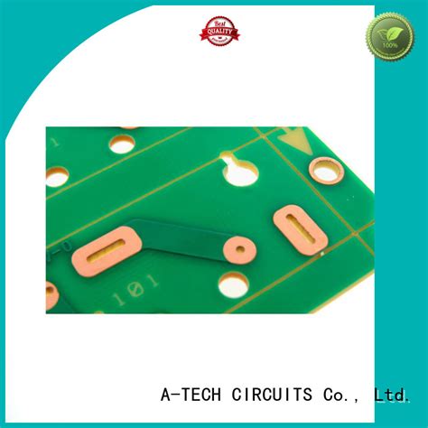
Castellated PCBs, also known as castellated hole PCBs or castellations, are printed circuit boards with special edge features that facilitate easy and secure connections between multiple boards. These features consist of plated half-holes or semicircular cutouts along the edges of the PCB, resembling the battlements of a castle, hence the name “castellated.”
Castellated holes offer several advantages over traditional connection methods, such as pin headers or connectors. They provide a low-profile, space-saving solution for board-to-board connections, making them ideal for compact electronic devices and modular designs.
How Castellated Holes Are Formed
The process of creating castellated holes on a PCB involves a combination of drilling, routing, and plating techniques. Here’s a step-by-step overview of how castellated holes are formed:
-
PCB Design: The PCB design is created using electronic design automation (EDA) software, incorporating the desired castellated hole features along the edges of the board.
-
Drilling: Once the PCB design is finalized, the fabrication process begins with drilling holes at the designated locations for the castellated holes. These holes are typically drilled using a computer numerical control (CNC) machine or a laser drill, ensuring precise positioning and consistent hole sizes.
-
Routing: After drilling, the PCB undergoes a routing process to create the semicircular cutouts that form the castellated holes. A specialized router bit is used to remove the excess material around the drilled holes, creating the characteristic half-hole shape.
-
Plating: The drilled and routed holes are then plated with a conductive material, usually copper, to establish electrical connectivity between the layers of the PCB. This plating process ensures that the castellated holes can function as reliable electrical connections.
-
Solder Mask Application: A solder mask is applied to the PCB, covering the areas that should not be exposed to solder during the assembly process. The solder mask is selectively applied, leaving the castellated holes exposed to allow for soldering.
-
Surface Finish: Finally, the PCB undergoes a surface finish process to protect the exposed copper and enhance solderability. Common surface finishes for castellated PCBs include immersion gold (ENIG), immersion silver, or organic solderability preservative (OSP).

Advantages of Castellated PCBs
Castellated PCBs offer several benefits over traditional connection methods, making them an attractive choice for various electronic applications. Some of the key advantages of castellated PCBs include:
-
Space Savings: Castellated holes provide a low-profile and compact solution for board-to-board connections, eliminating the need for bulky connectors or headers. This space-saving feature is particularly valuable in miniaturized electronic devices where every millimeter counts.
-
Simplified Assembly: Connecting multiple PCBs using castellated holes is a straightforward process. The boards can be easily aligned and soldered together, reducing assembly time and minimizing the risk of connection errors.
-
Enhanced Mechanical Strength: Castellated connections offer improved mechanical strength compared to traditional pin headers or connectors. The plated half-holes provide a larger surface area for soldering, resulting in a more robust and reliable connection between the boards.
-
Improved Signal Integrity: Castellated holes enable shorter signal paths between connected boards, reducing the potential for signal loss or interference. This is especially important in high-speed or high-frequency applications where maintaining signal integrity is critical.
-
Modular Design Flexibility: Castellated PCBs facilitate modular design approaches, allowing for easy interchangeability and customization of electronic modules. This modularity enables designers to create versatile and adaptable systems, simplifying upgrades and modifications.
-
Cost-Effectiveness: By eliminating the need for additional connectors or headers, castellated PCBs can reduce the overall component count and cost of an electronic assembly. Additionally, the simplified assembly process associated with castellated connections can lead to cost savings in manufacturing.

Applications of Castellated PCBs
Castellated PCBs find applications in a wide range of electronic products and industries. Some common applications include:
-
IoT Devices: Castellated PCBs are widely used in Internet of Things (IoT) devices, where compact sizes and modular designs are essential. They enable the integration of various sensors, wireless modules, and processing units into a single, space-efficient package.
-
Wearable Electronics: Wearable devices, such as smartwatches, fitness trackers, and medical monitoring systems, often rely on castellated PCBs for their compact and lightweight design requirements. Castellated connections allow for the efficient stacking and interconnection of multiple boards within the limited space available in wearable devices.
-
Automotive Electronics: In the automotive industry, castellated PCBs are used in various electronic control units (ECUs), sensors, and infotainment systems. The robust mechanical strength and reliable connections provided by castellated holes make them suitable for the demanding environmental conditions encountered in automotive applications.
-
Industrial Automation: Castellated PCBs are employed in industrial automation systems, such as programmable logic controllers (PLCs), human-machine interfaces (HMIs), and sensor modules. The modular nature of castellated connections enables easy customization and scalability of industrial control systems.
-
Consumer Electronics: Many consumer electronic products, including smartphones, tablets, and portable gaming devices, utilize castellated PCBs for their compact and modular designs. Castellated connections allow for the efficient integration of multiple functional modules, such as displays, cameras, and storage components.
-
Aerospace and Defense: In aerospace and defense applications, castellated PCBs are used in avionics systems, communication equipment, and ruggedized electronic devices. The space-saving and robust nature of castellated connections make them suitable for the stringent requirements of these industries.

Design Considerations for Castellated PCBs
When designing castellated PCBs, several factors must be considered to ensure optimal performance and manufacturability. Some key design considerations include:
-
Hole Size and Spacing: The size and spacing of the castellated holes should be carefully chosen based on the specific requirements of the application. Factors such as the desired current carrying capacity, mechanical strength, and available board space should be taken into account.
-
Plating Thickness: The plating thickness of the castellated holes is critical for ensuring reliable electrical connections and mechanical strength. Adequate plating thickness should be specified to withstand the stresses of soldering and normal operation.
-
Solder Mask Design: The solder mask design around the castellated holes should be optimized to prevent solder bridging and ensure proper solderability. Adequate solder mask clearance should be provided around the holes to allow for effective solder wicking and fillets.
-
Board Thickness: The thickness of the PCB should be considered when designing castellated holes. Thinner boards may require smaller hole sizes and tighter tolerances to maintain mechanical integrity and prevent breakage during assembly.
-
Signal Integrity: For high-speed or high-frequency applications, signal integrity considerations should be taken into account when designing castellated connections. Proper impedance matching, ground plane design, and trace routing techniques should be employed to minimize signal reflections and crosstalk.
-
Manufacturing Tolerances: The manufacturing tolerances for castellated holes should be carefully specified to ensure consistent and reliable connections. Tight tolerances may be necessary for high-precision applications, while looser tolerances may be acceptable for less critical designs.
Manufacturing and Assembly of Castellated PCBs
The manufacturing and assembly process for castellated PCBs involves several key steps to ensure the quality and reliability of the final product. Here’s an overview of the manufacturing and assembly process:
-
PCB Fabrication: The castellated PCB is fabricated using standard PCB manufacturing techniques, including drilling, routing, plating, and solder mask application, as described earlier.
-
Solder Paste Application: Solder paste is applied to the castellated holes and other components on the PCB using a stencil printing process. The solder paste consists of tiny solder particles suspended in a flux medium, which helps to facilitate the soldering process.
-
Component Placement: Surface mount components, including any mating PCBs with castellated edges, are placed onto the solder paste using automated pick-and-place machines or manual assembly techniques.
-
Reflow Soldering: The PCB Assembly undergoes a reflow soldering process, where the board is heated to a specific temperature profile in a reflow oven. The heat melts the solder paste, forming a strong mechanical and electrical connection between the components and the PCB.
-
Inspection and Testing: After the reflow soldering process, the assembLED PCB undergoes visual inspection and electrical testing to verify the quality of the soldered connections and ensure proper functionality. Automated optical inspection (AOI) systems or X-ray inspection may be used to detect any soldering defects or misalignments.
-
Cleaning and Protection: If necessary, the assembled PCB may undergo a cleaning process to remove any flux residues or contaminants from the surface. Conformal coating or potting may also be applied to protect the PCB and its components from environmental factors such as moisture, dust, or mechanical stress.
Frequently Asked Questions (FAQ)
-
What is the difference between castellated holes and plated through-holes?
Castellated holes are plated half-holes or semicircular cutouts along the edges of a PCB, while plated through-holes are fully enclosed holes that extend through the entire thickness of the board. Castellated holes are used for board-to-board connections, while plated through-holes are typically used for mounting through-hole components or providing electrical connectivity between layers. -
Can castellated PCBs be used for high-current applications?
Yes, castellated PCBs can be designed to handle high currents by specifying appropriate hole sizes, plating thicknesses, and copper weights. However, the current carrying capacity of castellated connections is generally lower than that of traditional power connectors or bus bars. -
Are there any limitations on the number of castellated holes that can be placed on a PCB edge?
The number of castellated holes that can be placed on a PCB edge depends on factors such as the board thickness, hole size, and spacing requirements. In general, the spacing between castellated holes should be sufficient to maintain mechanical strength and prevent solder bridging. The specific limitations should be discussed with the PCB manufacturer based on the project requirements. -
How do castellated PCBs compare to other board-to-board connection methods in terms of cost?
Castellated PCBs can be a cost-effective solution for board-to-board connections compared to using separate connectors or headers. By eliminating the need for additional components and simplifying the assembly process, castellated connections can help reduce overall system costs. However, the cost comparison may vary depending on the specific design requirements and production volume. -
Are there any special considerations for handling and storing castellated PCBs?
Castellated PCBs should be handled and stored with care to prevent damage to the delicate castellated edges. Proper packaging and transportation methods should be used to avoid physical damage during shipping and handling. In terms of storage, castellated PCBs should be kept in a clean, dry environment to prevent oxidation or contamination of the exposed copper surfaces.
Conclusion
Castellated PCBs offer a versatile and efficient solution for board-to-board connections in a wide range of electronic applications. By incorporating plated half-holes or castellations along the edges of the PCB, designers can achieve compact, low-profile, and mechanically robust connections between multiple boards.
The manufacturing process for castellated PCBs involves precise drilling, routing, and plating techniques to create the characteristic semicircular cutouts. Proper design considerations, such as hole size, spacing, and plating thickness, are essential to ensure optimal performance and manufacturability.
Castellated PCBs find applications in various industries, including IoT devices, wearable electronics, automotive systems, industrial automation, consumer electronics, and aerospace and defense. The space-saving, modular design flexibility, and cost-effectiveness of castellated connections make them an attractive choice for a wide range of electronic products.
As electronic devices continue to miniaturize and demand for modular designs grows, castellated PCBs are likely to play an increasingly important role in enabling compact, reliable, and efficient board-to-board connections.


Leave a Reply