Introduction to PCB Fabrication
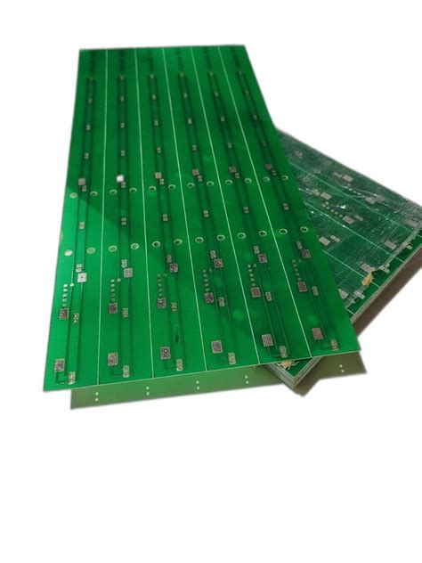
Printed Circuit Board (PCB) fabrication is the process of creating circuit boards that electrically connect electronic components using conductive pathways, tracks or signal traces etched from copper sheets laminated onto a non-conductive substrate. PCBs are at the heart of every electronic device we use today, from smartphones and laptops to medical equipment and aerospace technology.
The PCB fabrication process involves several key steps and techniques to turn a circuit design into a physical board. In this article, we’ll explore 10 essential PCB fabrication techniques every engineer and manufacturer should know to ensure high-quality, reliable circuit boards.
PCB Fabrication Process Overview
Before diving into specific techniques, let’s briefly review the overall PCB fabrication process:
- Design: Create the schematic diagram and PCB layout using EDA software
- Printing: Print the circuit pattern onto a transparent film or directly onto the PCB substrate
- Etching: Remove unwanted copper from the substrate, leaving only the desired circuit pattern
- Drilling: Drill holes for through-hole components and vias
- Plating: Apply a thin layer of metal (usually copper) to the holes to create electrical connections
- Soldermask Application: Apply a protective layer over the copper traces, leaving exposed areas for soldering
- Silkscreen: Print text and symbols onto the PCB for component placement and identification
- Surface Finish: Apply a final finish to protect exposed copper and enhance solderability
- Fabrication: Cut the panel into individual PCBs and perform final inspection
- Assembly: Solder components onto the PCB to create the final product
Now, let’s explore 10 crucial PCB fabrication techniques in detail.

1. Surface Mount Technology (SMT)
Surface Mount Technology (SMT) is a method of mounting electronic components directly onto the surface of a PCB. Unlike through-hole technology, where component leads are inserted into holes drilled in the board, SMT components have small metal tabs or pins that are soldered onto pads on the PCB surface.
Advantages of SMT:
- Smaller component sizes allow for denser PCB designs
- Faster assembly process due to automated pick-and-place machines
- Lower cost for high-volume production
- Improved mechanical performance due to reduced board size and weight
SMT Process Steps:
- Solder Paste Application: Apply solder paste to the component pads using a stencil or screen printing process
- Component Placement: Place SMT components onto the solder paste using pick-and-place machines or manual methods
- Reflow Soldering: Pass the PCB through a reflow oven to melt the solder paste and create a permanent connection between the components and pads
- Inspection: Perform visual and automated optical inspection (AOI) to ensure proper component placement and soldering quality
| Characteristic | Through-Hole Technology | Surface Mount Technology |
|---|---|---|
| Component Size | Larger | Smaller |
| PCB Density | Lower | Higher |
| Assembly Speed | Slower | Faster |
| Production Cost | Higher for low-volume | Lower for high-volume |
| Mechanical Performance | Robust | Improved due to smaller size |

2. Multilayer PCBs
Multilayer PCBs are circuit boards that consist of three or more conductive layers laminated together with insulating material between each layer. These boards allow for more complex designs and higher component density compared to single or double-layer PCBs.
Advantages of Multilayer PCBs:
- Increased circuit density and functionality in a smaller footprint
- Improved signal integrity and electromagnetic compatibility (EMC)
- Reduced electromagnetic interference (EMI) and crosstalk
- Better power and ground distribution
Multilayer PCB Fabrication Process:
- Inner Layer Etching: Etch the circuit patterns onto the inner layer copper foils
- Lamination: Stack and align the inner layers with insulating prepreg material between each layer, then laminate under heat and pressure
- Drilling: Drill through-holes and vias to create connections between layers
- Plating: Plate the drilled holes with copper to establish electrical connections
- Outer Layer Etching: Etch the circuit patterns onto the outer layer copper foils
- Soldermask and Silkscreen Application: Apply soldermask and silkscreen to the outer layers
- Surface Finish: Apply the final surface finish (e.g., HASL, ENIG, or OSP) to protect the exposed copper and facilitate soldering
| Layer Count | Typical Applications |
|---|---|
| 1-2 | Simple circuits, low-density designs |
| 4 | General-purpose digital and analog circuits |
| 6-8 | Complex digital circuits, high-speed designs |
| 10+ | High-density interconnect (HDI), advanced packaging |

3. High Density Interconnect (HDI)
High Density Interconnect (HDI) is a PCB fabrication technique that involves creating very fine circuit features and micro-vias to achieve higher component density and improved signal integrity. HDI PCBs are commonly used in smartphones, wearables, and other compact electronic devices.
Key Features of HDI PCBs:
- Fine line width and spacing (typically less than 100 μm)
- Blind and buried micro-vias for inter-layer connections
- Thin dielectric materials for reduced layer thickness
- Sequential lamination process for building up multiple layers
HDI PCB Fabrication Process:
- Build-up: Create the inner layers using standard PCB fabrication techniques
- Micro-via Drilling: Drill blind and buried micro-vias using laser or mechanical drilling methods
- Plating: Plate the micro-vias with copper to create electrical connections
- Lamination: Laminate additional layers with insulating material and repeat the build-up process as needed
- Outer Layer Processing: Etch the outer layer circuit patterns, apply soldermask and silkscreen, and apply the final surface finish
| HDI Class | Line Width/Spacing | Micro-Via Diameter |
|---|---|---|
| Class 1 | 100-75 μm | 150-100 μm |
| Class 2 | 75-50 μm | 100-50 μm |
| Class 3 | 50-30 μm | 50-30 μm |
4. Flexible PCBs
Flexible PCBs, also known as flex circuits, are thin, lightweight, and bendable circuit boards made from flexible plastic substrates such as polyimide or polyester. Flex PCBs are ideal for applications that require compact packaging, motion, or repeated flexing, such as wearable devices, medical equipment, and automotive electronics.
Advantages of Flexible PCBs:
- Conformability to fit into tight spaces or curved surfaces
- Reduced weight and thickness compared to rigid PCBs
- Improved reliability in applications with vibration or repeated flexing
- Simplified assembly process by replacing multiple rigid boards and connectors with a single flex circuit
Flexible PCB Fabrication Process:
- Substrate Preparation: Clean and treat the flexible substrate to improve adhesion
- Copper Lamination: Laminate copper foil onto the flexible substrate using adhesive or heat and pressure
- Circuit Patterning: Create the circuit pattern using photolithography and etching processes
- Cover Layer Application: Apply a protective cover layer over the circuit pattern, leaving exposed areas for soldering
- Drilling and Cutting: Drill holes for through-hole components and cut the flex PCB to its final shape
- Surface Finish: Apply the final surface finish (e.g., ENIG or OSP) to protect the exposed copper and facilitate soldering
| Characteristic | Rigid PCB | Flexible PCB |
|---|---|---|
| Substrate Material | FR-4, Polyimide | Polyimide, Polyester |
| Thickness | 0.8-3.2 mm | 0.05-0.2 mm |
| Weight | Higher | Lower |
| Conformability | Limited | High |
| Vibration Resistance | Lower | Higher |
5. Controlled Impedance
Controlled impedance is a PCB fabrication technique used to manage the impedance of transmission lines in high-speed digital circuits. By carefully controlling the geometry and materials of the PCB traces, designers can ensure proper signal integrity and minimize reflections, crosstalk, and electromagnetic interference (EMI).
Factors Affecting Impedance:
- Trace width and thickness
- Dielectric material properties (dielectric constant and thickness)
- Trace spacing and geometry
- Proximity to ground or power planes
Controlled Impedance PCB Fabrication Process:
- Impedance Calculation: Use PCB design software or calculators to determine the required trace geometry and spacing for the target impedance
- Material Selection: Choose PCB materials with consistent dielectric properties to ensure predictable impedance
- Fabrication Process Control: Tightly control the PCB fabrication process to maintain consistent trace geometry and dielectric thickness
- Impedance Testing: Perform impedance testing on sample PCBs to verify that the actual impedance matches the target value
- Adjustments and Fine-tuning: Make necessary adjustments to the fabrication process or design to achieve the desired impedance
| Impedance Type | Typical Applications |
|---|---|
| 50 Ω | RF circuits, high-speed digital interfaces (e.g., USB, HDMI) |
| 75 Ω | Video circuits, coaxial cables |
| 90-120 Ω | Differential pair signaling (e.g., PCIe, Ethernet) |
6. Blind and Buried Vias
Blind and buried vias are specialized types of interconnects used in multilayer PCBs to create connections between inner layers without penetrating the entire board. This technique allows for higher component density, improved signal integrity, and more compact PCB designs.
Types of Vias:
- Through Vias: Connect all layers of the PCB, from top to bottom
- Blind Vias: Connect an outer layer to one or more inner layers, but do not penetrate the entire board
- Buried Vias: Connect two or more inner layers without reaching either outer layer
Blind and Buried Via Fabrication Process:
- Inner Layer Processing: Create the inner layer circuit patterns and drill the blind or buried vias
- Lamination: Laminate the inner layers with prepreg material, aligning the vias as needed
- Drilling: Drill through-holes to connect the outer layers to the inner layers (for blind vias) or to create connections between all layers (for through vias)
- Plating: Plate the drilled holes and vias with copper to establish electrical connections
- Outer Layer Processing: Complete the outer layer processing steps, including soldermask and silkscreen application
| Via Type | Layers Connected | Fabrication Complexity |
|---|---|---|
| Through | All layers | Low |
| Blind | Outer to inner | Medium |
| Buried | Inner to inner | High |
7. Via-in-Pad
Via-in-Pad is a PCB fabrication technique where a via is placed directly within a component pad, allowing for more compact PCB designs and improved signal integrity. This technique is particularly useful in high-density designs, such as Ball Grid Array (BGA) packages, where space is limited.
Advantages of Via-in-Pad:
- Reduced PCB size by eliminating the need for additional routing space
- Improved signal integrity by minimizing the distance between the component and the via
- Better thermal management by providing a direct path for heat dissipation
- Enhanced manufacturing efficiency by simplifying the assembly process
Via-in-Pad Fabrication Process:
- Pad and Via Design: Design the component pads with vias placed directly within the pad area
- Drilling: Drill the vias using a small-diameter drill bit
- Plating: Plate the vias with copper to create electrical connections
- Filling: Fill the vias with a non-conductive epoxy or conductive paste to create a smooth surface for component placement
- Outer Layer Processing: Complete the outer layer processing steps, including soldermask and silkscreen application
| Via-in-Pad Type | Filling Material | Advantages |
|---|---|---|
| Non-conductive | Non-conductive epoxy | Lower cost, easier to process |
| Conductive | Conductive paste | Improved thermal and electrical performance |
8. Microvias
Microvias are small-diameter vias used in HDI PCBs to create high-density interconnects between layers. These vias are typically fabricated using laser drilling or photolithography techniques, allowing for via diameters smaller than 150 μm.
Advantages of Microvias:
- Higher interconnect density compared to traditional mechanically-drilled vias
- Improved signal integrity due to reduced via size and parasitic effects
- Better power and ground distribution in high-density designs
- Enables the use of fine-pitch components, such as chip-scale packages (CSPs) and μBGAs
Microvia Fabrication Process:
- Photolithography: Create a photoresist pattern defining the microvia locations
- Laser Drilling: Drill the microvias using a focused laser beam
- Desmear: Remove any remaining debris or resin from the microvia holes
- Plating: Plate the microvias with copper to create electrical connections
- Filling: Optionally, fill the microvias with a non-conductive epoxy or conductive paste to create a smooth surface for subsequent layers
| Microvia Type | Diameter Range | Aspect Ratio |
|---|---|---|
| Type I | 50-150 μm | 1:1 |
| Type II | 50-150 μm | 1:1 – 1:2 |
| Type III | 25-50 μm | 1:1 – 1:2 |
9. Embedded Components
Embedded components are a PCB fabrication technique where passive components, such as resistors and capacitors, are embedded within the layers of a multilayer PCB. This technique offers several advantages over traditional surface-mounted components, including reduced board size, improved electrical performance, and enhanced reliability.
Advantages of Embedded Components:
- Reduced PCB size and thickness by eliminating the need for discrete surface-mounted components
- Improved signal integrity and reduced parasitic effects due to shorter interconnects
- Enhanced reliability by protecting components from environmental factors and mechanical stress
- Simplified assembly process and reduced component count
Embedded Component Fabrication Process:
- Component Preparation: Prepare the embedded components by applying terminations and protective coatings as needed
- Inner Layer Processing: Create the inner layer circuit patterns and place the embedded components in their designated locations
- Lamination: Laminate the inner layers with prepreg material, encapsulating the embedded components
- Drilling: Drill through-holes and vias to create connections to the embedded components
- Plating: Plate the drilled holes and vias with copper to establish electrical connections
- Outer Layer Processing: Complete the outer layer processing steps, including soldermask and silkscreen application
| Embedded Component Type | Typical Values | Applications |
|---|---|---|
| Resistors | 1 Ω – 1 MΩ | Pull-up/down, termination |
| Capacitors | 1 pF – 1 μF | Decoupling, filtering |
| Inductors | 1 nH – 100 nH | RF circuits, impedance matching |
10. 3D Printed Electronics
3D printed electronics is an emerging PCB fabrication technique that combines additive manufacturing (3D printing) with conductive materials to create functional electronic circuits and components. This technology enables rapid prototyping, customization, and the creation of complex, three-dimensional structures that are difficult or impossible to achieve with traditional PCB fabrication methods.
Advantages of 3D Printed Electronics:
- Rapid prototyping and iteration of PCB designs
- Customization and personalization of electronic devices
- Creation of complex, three-dimensional structures and non-planar circuits
- Integration of electronics with mechanical components in a single, unified structure
- Potential for reduced waste and environmentally-friendly production
3D Printed Electronics Fabrication Process:
- Design: Create a 3D model of the electronic circuit or component using CAD software
- Material Selection: Choose a suitable 3D printing material (e.g., conductive filament, conductive ink) and a compatible 3D printer
- Printing: Print the 3D structure using the selected material and printer
- Post-processing: Perform any necessary post-processing


Leave a Reply