Introduction to PCBs
A printed circuit board (PCB) is a board made of insulating material like FR4 fiberglass with thin copper foil laminated onto it. The copper layer is patterned to form conductive tracks and pads that electrically connect various components mounted on the board. PCBs serve as the structural framework to support and connect electronic components without separate wires. They are at the heart of all electronic devices and equipment we use.
PCBs were first developed in the 1930s but became more widespread from the 1950s. Some key advantages of using PCBs over traditional wire assemblies are:
- Compact design enabling miniaturization
- Improved reliability and ruggedness
- Consistent quality with mass production
- Simplified assembly and servicing
- Reproducible and scalable manufacturing
PCB Production Process Overview
PCB production involves complex processes to fabricate a multi-layered board with conductive copper traces on the surface to mount and interconnect components. It consists of four major steps:
1. Design
The PCB layout is designed by an engineer based on circuit requirements using CAD software. The layout data is converted to manufacturing files.
2. Fabrication
This involves sequentially creating conductive layers and laminating them to produce a multi-layer PCB with the designed layout.
3. Assembly
Electronic components are soldered onto the fabricated PCB to form a functional printed circuit assembly (PCA).
4. Testing
The bare PCB and assembled board are tested for defects and functionality at multiple stages.
We will look at PCB fabrication, assembly and testing stages in more detail.
PCB Fabrication Process
PCB fabrication transforms the digital layout into a physical board ready for component mounting. For multi-layer boards, it involves creating individual metal layers and laminating them together. The key steps are:
1. Inner Layer Fabrication
The inner layers (buried layers) are fabricated first. A copper clad FR4 laminate is coated with photoresist and imaged with the layout pattern. The resist is developed and unwanted copper etched away leaving only the desired tracks.
Multiple such etched laminates are created depending on the layer count of the final PCB. Alignment holes are drilled for layer alignment.
2. Lamination Stacking
The etched inner layers are stacked alternately with prepreg adhesive layers. Prepreg is glass fabric partially cured with epoxy resin. Layers are arranged so that core dielectric separates copper layers.
3. Lamination Pressing
The layer stack is laminated under heat and pressure in a hydraulic press. The resin in the prepreg layers flows and cured into a solid board with strong bonding between layers.
Typical parameters are 175°C temperature, 200 psi pressure for 90 minutes. Cooling under pressure prevents warpage.
4. Outer Layer Fabrication
After lamination, the board has a continuous copper layer on the outer surfaces. Photolithography process is used again to form the desired outer layer circuit pattern. This completes the conductive layer fabrication.
5. Drilling
Holes are drilled at locations where components are to be mounted. For multi-layer boards, drilling is done before outer layer patterning so buried vias are formed.
6. Plating and Coating
The holes are plated with copper to form a conductive barrel. Solder mask and silkscreen coatings are applied. The boards are now ready for PCB assembly.
PCB Assembly Process
This involves soldering components onto the fabricated PCB and transforming it into a functional electronic circuit assembly. The key steps are:
1. Screen Printing
Solder paste is screen printed onto the PCB pads where components are to be placed. This temporarily fixes components.
2. Component Placement
Components are accurately placed onto the PCB according to the bill of materials (BOM) using automated pick and place machines.
3. Reflow Soldering
The PCB with components is passed through a reflow oven with a temperature profile. The solder paste melts, wets pads and leads, then solidifies to form solder joints fixing the components.
4. Cleaning
Any residual flux is cleaned from the soldered board using suitable cleaning agents to avoid corrosion.
5. Conformal Coating
A protective plastic coating may be applied over the assembled board leaving only connectors exposed.
6. Functional Testing
The fully assembled PCB is electrically tested to validate functionality. Failed boards are reworked or discarded.
PCB Testing
Testing is integral throughout PCB production to catch any defects and avoid assembling bad boards. Testing steps include:
Bare Board Testing
This is done after fabricating the bare PCB before assembly:
- Automated optical inspection (AOI) checks for visible defects and abrasions.
- Net connectivity testing uses flying probe or fixture methods to validate electrical connectivity of traces.
- In-circuit testing checks for short circuits, opens, leakage between circuits.
- x-ray inspection reveals hidden layer defects.
Assembled Board Testing
This is done after populating components:
- AOI inspection checks component presence and orientation, solder joint quality.
- In-circuit testing validates electrical functioning of circuits.
- Flying probe testing checks interconnects between components.
- Functional testing verifies the board behavior based on its specifications.
Advanced PCB Production Technologies
Advancements in PCB production capabilities enable denser, higher performance boards critical for modern electronics:
Photolithography
Finer line width and spacing down to 25μm tracks are achieved using advanced photoresists, laser direct imaging, and high accuracy metal etching.
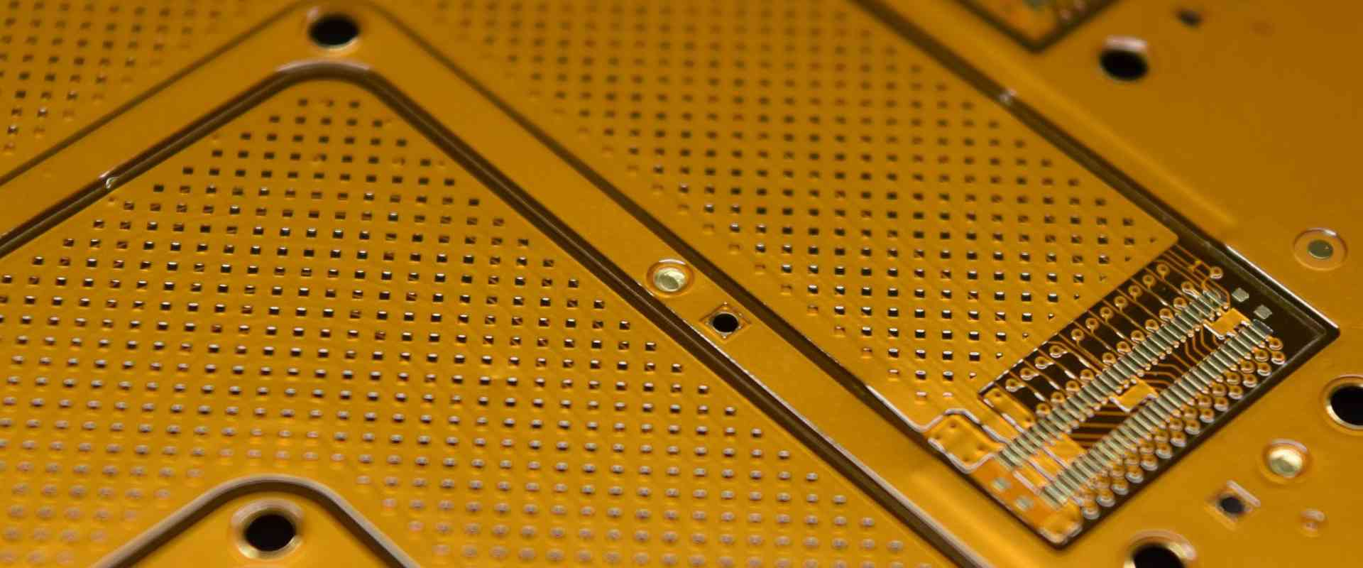
High Density Interconnects
Microvias, buried and stacked vias, blind and filled vias allow greater interconnect density.
High Layer Count
Improved lamination processes permit over 20-30 conductive layers interconnected vertically.
HDI Technology
Laser microvia PCBs with tighter interconnects facilitate complex high density designs.
Embedded Passives
Passive components like resistors and capacitors are built into the PCB itself, saving space.
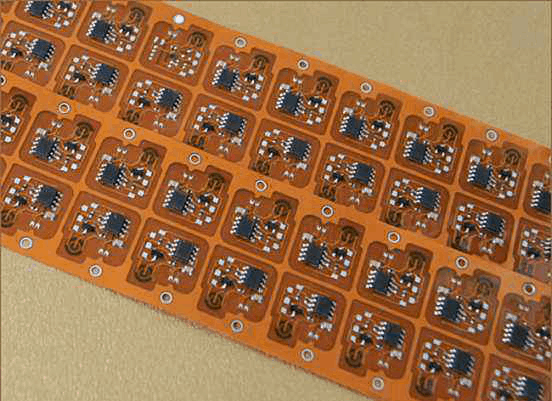
Flexible Circuits
Flexible substrates like polyimide allow bendable PCBs for wearables and compact devices.
Rigid-Flex
Combination of rigid and flexible sections in one board enables 3D packaging.
Factors Affecting PCB Production Time
The time required to produce a batch of PCBs depends on several factors:
- Board complexity – layer count, pad/track density, fine features
- Board size – smaller boards can be panelized for faster production
- Quantity – setup time is fixed so larger quantities have smaller time/board
- Lead-time for raw materials – can range from days to weeks
- Testing and inspection requirements
- Production yield and rework rate
- Manufacturer’s current workloads and capacity
As a guideline, the fabrication time ranges from:
- 2-3 days for simple double-sided boards
- 5-7 days for moderately complex 6-8 layer boards
- 8-10 days for high layer counts (16+) and advanced board technologies
But actual production times can vary significantly from the above. Assembly adds 1-2 days, but can often be done in parallel with fabrication to optimize lead time.
Factors Affecting PCB Production Costs
The costs involved in PCB production include:
- Material – raw PCB substrate, copper foil, soldermask, etc.
- Labor – operators, engineers, management overhead
- Equipment – for processes like photolithography, drilling, lamination, etc.
- Tooling – fabrication of masks, test fixtures
- Testing – bare board testing and assembled board functional test
- Floor space and facility expenses
- Energy and consumables
The main factors affecting overall PCB cost:
- Board size – larger boards use more raw materials
- Layer count – each layer addition increases cost
- Production quantity – cost per board drops with larger quantity
- Fine features – high density interconnects require advanced processes
- Special materials – alternative substrates drives costs higher
- Component density – more components need miniaturization
- Functionality testing – adds time and cost
- Reworks of defective boards
- Location of production facility – labor and operational costs
Frequently Asked Questions
How are very high density PCBs with small tracks/spaces fabricated?
Special photolithography techniques like laser direct imaging and advanced chemical processes allow patterning of extremely fine tracks down to 25 microns spacing. Plating technology can deposit copper tracks of similar widths. The boards usually use microvias and often incorporate blind or buried vias.
What are the different PCB assembly technologies?
The main assembly technologies are:
- Through-hole assembly – leads inserted into holes
- Surface mount technology (SMT) – components soldered onto pads
- Chip-on-board (COB) – bare dies directly bonded
- Flip-chip – direct attachment of inverted chips
Currently over 95% of components are assembled using SMT.
How are multi-layer PCBs aligned properly during stacking?
Tooling holes are drilled at specific locations in the individual layers. These fit onto precision alignment pins in the layup fixture. This ensures exact registration between layers during stacking before lamination. Lasers may also be used to align layers by optically detecting fiducials.
What are the standard PCB substrate thicknesses available?
Common FR4 glass-epoxy core thicknesses are:
- 0.4 mm
- 0.8 mm
- 1.0 mm
- 1.6 mm
- 2.0 mm
- 2.4 mm
Prepreg adhesive layers are usually around 0.1 mm thick. Core thickness above 3mm is rare in modern PCBs.
How is impedance controlled in PCB traces?
Impedances like 50Ω are maintained by matching the PCB trace width to the substrate dielectric constant based on formulas. The trace is routed over a continuous ground plane which serves as the return path. The trace geometry and ground clearance govern impedance.


Leave a Reply