Introduction
A printed circuit board (PCB) is made up of layers of conductive and insulating materials stacked on top of each other. The sequence and thickness of these layers is referred to as the PCB layer stackup. The layer stackup defines the electrical, mechanical, and thermal characteristics of the PCB. Selecting the optimal layer stackup is crucial for designing a reliable PCB that meets performance requirements within budget constraints.
This article provides an overview of PCB layer stackup – what the different layers are, how they are organized, key design considerations, and common stackup configurations. We’ll also look at the role of layer stackup in signal integrity, EMI control, and thermal management.
PCB Layer Types
The core layers in a PCB stackup are:
1. Copper Layers
These are thin sheets of copper foil that are patterned to form the conductive traces and planes. Copper thickness typically ranges from 1/2 oz (17 μm) to 3 oz (105 μm) per square foot. The copper layers are where components are mounted and all the electrical connectivity is formed.
2. Dielectric Layers
Dielectric or insulating materials separate the copper layers. Common dielectrics are FR-4, polyimide, and ceramic. Dielectrics electrically isolate between copper layers and provide mechanical rigidity to the PCB.
3. Soldermask Layers
The soldermask is a coat of polymer layer on the outer copper layers. It protects exposed copper from oxidation and prevents solder bridges between pads during assembly.
4. Silkscreen Layer
Used to print component outlines, markings, and board information for assembly and servicing.
In addition to the above, some PCBs may also integrate special purpose layers like buried/blind vias, embedded components, graphite core, metal core, etc.
Functions of PCB Layers
The four common PCB layer types are strategically organized within the stackup to fulfill the following key functions:
- Power distribution – power and ground planes
- Signal routing – signal traces carrying digital, analog, radio frequency (RF) signals.
- Controlled impedance – matched trace width, spacing and adjacent dielectric constant. Important for high speed traces.
- Shielding – ground planes between or around critical traces. Prevents EMI and crosstalk.
- Heat dissipation – thermal vias transferring heat to metal core or external layers.
Segregating the layers by function optimizes electrical performance and PCB reliability.
Key Design Considerations
Below are some key factors to consider when designing the layer stackup:
- Signal types – segregate digital, analog and RF signals. Prevent crosstalk.
- Route density – distribute routing across layers to prevent congestion.
- Impedance control – ensure consistent dielectric thickness around critical traces.
- High speed traces – place next to reference planes for controlled impedance.
- Power distribution – use entire layers or split power and ground planes.
- Shielding – sandwich critical signals between ground planes.
- EMI control – ensure adequate shielding and prevent slot antennas.
- Thermal vias – place heat generating components over thermal vias.
- Manufacturability – account for capabilities of board shop.
- Cost – optimize layer count and material choices.
Careful stackup design greatly improves signal and power integrity while minimizing EMI emissions. This leads to a robust PCB with first-pass success.
Typical Layer Stackup Configurations
Here are some typical layer stackup arrangements from simple to complex PCBs:
2 Layer Board
- Minimal cost
- Typically used for low complexity circuits
- Signal routing limited to 2 layers
4 Layer Board
- Low cost
- Provides good separation between signals and power
- Workhorse stackup for many PCBs
6 Layer Board
- Medium complexity circuits
- 2 signal layers between power and ground provides shielding
- Additional signal layers reduces congestion
8 Layer Board
- High speed signals isolated between ground planes
- 4 signal layers reduces congestion
- More power planes reduces noise
>8 Layer High Density Board
- Advanced circuits like network/graphics cards
- High layer count provides extensive routing and shields
- Integrates many power planes, differential pairs, impedance control
As you can see, the layer stackup complexity increases with PCB density and performance requirements. High speed signals need reference planes for controlled impedance. Multiple voltage rails require dedicated power planes. The stackup must also provide adequate isolation and shielding between critical nets.
Impact on Signal Integrity
Layer stackup design is integral to maintaining signal integrity in high speed PCBs. Some key factors:
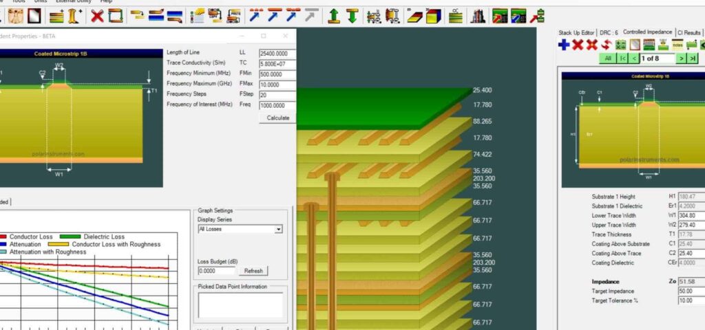
Reference planes – Each high speed signal trace needs to run next to a continuous reference plane. This establishes a controlled impedance environment. Reference planes also shield the traces from EMI.
Differential pairs – For really high speed signals, differential pairs are used. Each trace in the pair needs to be routed over its own uninterrupted reference plane.
Isolation – High speed traces should be isolated from aggressor signals. Placing ground planes between signal layers provides a shield. Voids in the planes can degrade shielding.
Dielectric consistency – The dielectric thickness on either side of a trace impacts its impedance. Any variations can lead to impedance discontinuities and reflections.
Paying attention to layer stackup minimizes discontinuities, crosstalk, and EMI – enabling high speed signals to transmit reliably from their source to destination.
EMI Control Through Layer Stackup
A good PCB layer stackup facilitates EMI control in multiple ways:
Reference planes – Continuous reference planes next to signals prevent emissions from leaking out. They also block external fields from disrupting traces.
Shielding – Strategic placement of ground planes between or around critical signals confines EMI within the board sandwich.
Voids – Reference plane voids can act like slot antennas allowing EMI leakage. Solid planes are ideal for shielding.
Decoupling – Multiple localized power planes with interlayer decoupling capacitors aid power distribution while lowering loop inductance.
Transmission lines – Controlled impedance traces matched to their terminations absorb signals preventing reflections and emissions.
Noisy layers – Keeping switch mode power supplies and other noisy circuits in the inner layers prevents emissions.
Component placement – Group radiating components in shielded sections with local filtering to contain EMI.
An optimized layer stackup keeps EMI contained within the board and protects sensitive signals from external interference.
Thermal Management Through Layer Stackup
Here are some techniques to enhance thermal management through PCB layer stackup design:
Thermal vias – Vias transfer heat from inner layers to the external layers where it can dissipate. Place vias underneath major heat sources.
Ground planes – Uninterrupted ground planes conduct heat laterally to spread heat uniformly before it dissipates.
Metal core – A metal core like aluminum or copper sandwiched in the stackup spreads heat evenly like a heat sink.
Thermal pads – Expose large copper pads on the outer layers to transfer component heat outward.
Heatsinks and clips – Heatsinks over components pull heat away. Spring clips enhance thermal transfer to the board.
Thermally conductive dielectric – Dielectrics like aluminum oxide ceramic rapidly conduct heat laterally.
Component placement – Ensure adequate cooling pathways around heat generating components.
No voids – Reference plane voids act as thermal barriers. Use thermally conductive vias to bypass voids.
Good stackup thermal design keeps components safely below temperature limits for reliable operation.
Conclusion
The PCB layer stackup underpins electrical, thermal and EMI characteristics of the board through careful arrangement of material layers. For complex high speed designs, the stackup must isolate critical signals, provide low inductance power distribution, shield EMI, and conduct heat – all while maintaining cost constraints. A good grasp of stackup design principles coupled with circuit analysis and modeling helps define an optimal stackup tailored to application needs.
FAQ
Q: What is the standard PCB dielectric material?
A: The most common dielectric material used in PCBs is FR-4 glass epoxy. It provides good mechanical strength and electrical performance at a reasonable cost. Typical FR-4 thickness is 0.062″ (1.6 mm). Higher frequency boards may use advanced dielectrics like polyimide or PTFE. Ceramic based PCBs are also used but are more expensive.
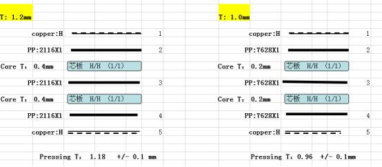
Q: What is the difference between core, prepreg and bondply dielectric?
A: Core dielectric is the main insulating substrate laminated between copper foil layers. Prepreg is partially cured resin coated on the core layers to glue the stack together. Bondply is a super thin prepreg to bond outer foil layers to the core stackup without adding significant thickness.
Q: How many routing layers are needed for a complex PCB?
A: There is no fixed rule on the number of layers. It depends on component density, routing constraints, signal types, and other performance requirements. Typically 8-12 layers is sufficient for complex double-sided boards. High density boards like GPUs can go up to 24 layers or more.
Q: Are all layers in a PCB stackup required to be the same dielectric material?
A: No, the dielectric material can be different for core, prepreg and bondply layers based on design needs. Critical high speed signals may route between polyimide prepregs for lower loss, while other sections can use standard FR-4. Mixed dielectric stackups help optimize cost and performance.
Q: Can traces be routed on the outer soldermask layer of a PCB?
A: No, the soldermask layer is a thin coating not intended for routing traces. It is applied over the copper layer merely for insulation and marking. Traces are routed only on the copper layers internal to the stackup.


Leave a Reply