Introduction
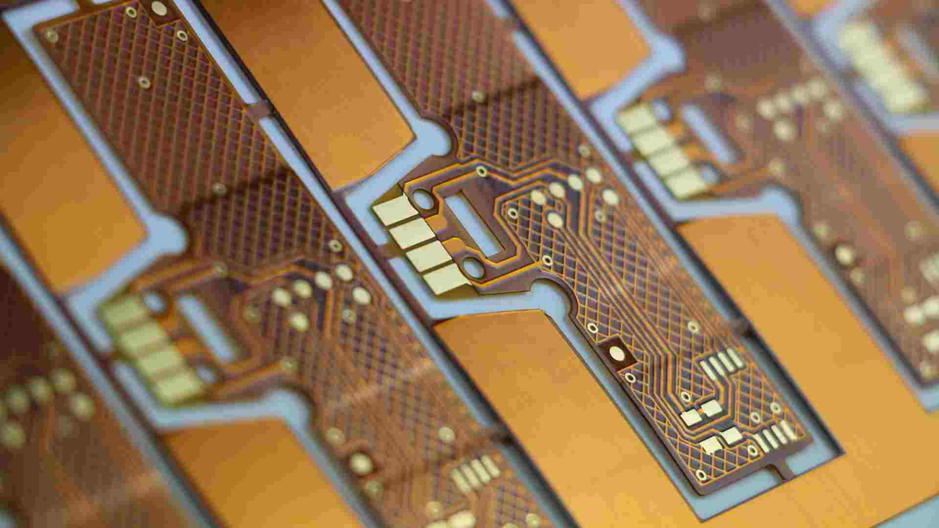
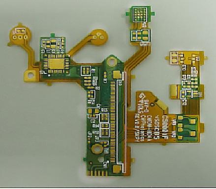
Flexible printed circuit boards (flex PCBs) are a type of printed circuit board that can bend and flex. They are made of flexible insulating substrate materials like polyimide or polyester rather than rigid materials like FR-4. Flex PCBs are useful for applications where flexibility, space savings, or fatigue resistance are required. They are commonly used in consumer electronics, automotive, aerospace, medical devices and more.
When designing a flex PCB, there are specific design rules that need to be followed to ensure proper functionality and manufacturability. In this article, we will take a deeper look at flex PCB design rules including trace widths, spacing, bending radius, layer stackup and more. Following these guidelines will result in a robust and reliable flex circuit.
Trace Width and Spacing
One of the most important flex PCB design rules is determining appropriate trace widths and spacing. Trace widths on flex circuits are generally thinner than rigid PCBs. Thinner traces allow for increased flexibility and improved reliability under dynamic bending. Here are typical trace width guidelines:
- External traces (outer layers): 0.10mm – 0.15mm
- Internal traces (inner layers): 0.075mm – 0.1mm
- Minimum trace width: 0.05mm
- Minimum spacing between traces: 0.075mm
Wider trace widths are possible but flexibility will be reduced. In high current applications, wider traces can be used to maintain ampacity.
It is also important to provide adequate spacing between traces, typically 2-3 times larger than the trace width. This prevents shorts and allows for flexibility. In dense designs, a minimum spacing of 0.075mm is recommended.
Bending Radius
The bending radius is an important parameter that determines the minimum bend a flex PCB can handle without damage. A smaller bending radius allows for tighter folds while a larger radius provides more robustness. Typical bending radius guidelines:
- Minimum bending radius: 3-5 times the total board thickness
- Dynamic/repeated bending: 10-20x board thickness
- Static bending: 2-3x board thickness
Sharp bends with a tight radius can crack traces or the polyimide base material. For applications with dynamic or repeated bending, increase the minimum radius. Use radius corners instead of 90 degree bends to reduce stress.
Layer Stackup
Flex PCBs can be designed with multiple conductive layers separated by flexible dielectric materials. A typical flex board may have 2 to 8 conductive layers. Here are some layer stackup guidelines:
- Place power and ground layers adjacent to each other to provide decoupling capacitance
- Do not place unsupported traces over voids in plane layers as they can crack under bending
- Stagger the edges of plane layers to avoid stair-stepping which causes mechanical weakness
- Use thicker dielectric materials between layers to provide increased separation and prevent shorts
Poor layer stackup choices can lead to mechanical failures and electrical issues. Work closely with your flex PCB manufacturer on optimal layer configurations.
Stiffeners and Shielding

In certain areas, stiffeners and shields can be added to flex circuits to provide mechanical support, heat dissipation and EMI shielding. Common stiffener materials include polyimide, aluminum, copper, FR-4. Guidelines include:
- Place stiffeners near connectors or along edges to prevent flexing damage
- Use thermal vias under components that generate heat
- Keep stiffeners small and isolated to avoid decreasing overall flexibility
- Use adhesive or mechanical fasteners to attach stiffeners and shields
Properly designed stiffeners and shields allow for enhanced performance without compromising bendability.
Component Selection
The selection of components is also an important consideration for flex PCB design:
- Prefer small surface mount devices over large through-hole components
- Use flexible or ultra-thin components when possible
- Avoid tall components that could fracture under bending
- Properly anchor larger components to prevent detachment during flexing
- Use flat lead terminations instead of formed leads
Choosing the right low-profile components suitable for dynamic environments will improve reliability.
Routing Features
There are also some routing guidelines that are specific to flex PCBs:
- Avoid 90 degree angles – use rounded corners instead
- Route traces perpendicular to the bend axis when crossing flex hinge areas
- Use zig-zag or serpentine patterns for traces over high stress areas
- Minimize the number of layers with traces over bend areas
- Ensure adequate trace widths for high current paths
- Seal exposed traces/pads to prevent oxidation over flex life
Smart routing over hinges and high stress zones will prevent conductor cracks.
Testing and Prototyping
Throughout the design process, testing and prototyping should be conducted to verify functionality under bending and dynamic conditions. Items to evaluate:
- Visual inspection for signs of conductor or base material cracks
- Continuity testing for opens/shorts after repeated bending cycles
- Signal integrity analysis and testing over the required motion range
- Mechanical cycling to validate robustness and component adhesion
- Shock and vibration testing for stringent applications
Finding design issues early through testing saves time and cost by avoiding unexpected failures down the road.
Summary
Designing reliable flex PCBs requires attention to special rules regarding trace spacing, bending radius, layer stackup, component selection, routing practices and design validation through testing. Working closely with an experienced flex PCB manufacturer is highly recommended to leverage their knowledge in designing cost-effective and robust flex circuits for your application. Following best practices for flex PCB design will ensure you avoid common pitfalls.
Frequently Asked Questions (FAQ)
Here are some common questions regarding flex PCB design rules:
Q: What are the minimum trace width and spacing I can use on a flex PCB?
A: Typical minimum trace widths are 0.05 mm to 0.1 mm, and minimum spacing is around 0.075 mm. However, it’s recommended to use wider traces and greater spacing when possible.
Q: How do I prevent cracking issues on flex PCBs?
A: Use generous bend radii, route traces perpendicular to bend axis, utilize zig-zag/serpentine traces, minimize trace layers over bends, and seal exposed traces.
Q: Can I use through-hole components on a flex PCB?
A: It’s better to avoid through-hole components. Opt for surface mount devices with flat leads. This avoids cracking issues under bending.
Q: What materials are commonly used for stiffeners and shields on flex PCBs?
A: Common materials include polyimide, aluminum, copper, and FR-4. Use thermally conductive interface material when attaching shields.
Q: What testing should I perform to validate flex PCB designs?
A: Conduct inspection for cracks, continuity testing, signal integrity analysis, mechanical cycling, shock/vibration testing, and temperature cycling based on the application.


Leave a Reply