Introduction to USB PCB
USB (Universal Serial Bus) is a widely used interface for connecting various peripheral devices to computers and other electronic devices. USB PCBs (Printed Circuit Boards) are essential components in the design and manufacturing of USB devices. They provide the necessary circuitry and connections for data transfer and power supply between the USB device and the host system.
However, designing and manufacturing USB PCBs can present several challenges. In this article, we will explore the common problems you may encounter when working with USB PCBs and provide solutions to overcome these issues.
Common Problems with USB PCBs
1. Signal Integrity Issues
Signal integrity is a critical aspect of USB PCB design. USB signals are high-speed and susceptible to noise, crosstalk, and signal reflections. These issues can lead to data corruption, communication errors, and device malfunctions.
Solutions:
- Ensure proper impedance matching between the USB traces and the connectors.
- Use differential pair routing techniques to minimize crosstalk and maintain signal integrity.
- Implement adequate ground planes and power planes to reduce noise and provide a stable reference.
- Follow the USB standard’s guidelines for trace width, spacing, and length.
2. Power Management Challenges
USB devices often rely on the USB bus for power supply. Managing power efficiently and ensuring stable power delivery can be challenging, especially for devices with high power requirements.
Solutions:
- Use voltage regulators and power management ICs to regulate and stabilize the power supply.
- Implement proper decoupling capacitors near the power pins to minimize noise and voltage fluctuations.
- Consider using separate power planes for analog and digital sections to reduce interference.
- Adhere to the USB standard’s power specifications and limitations.
3. Electromagnetic Interference (EMI)
USB devices can be sources of electromagnetic interference (EMI) or be susceptible to external EMI. EMI can cause signal degradation, data errors, and compliance issues with regulatory standards.
Solutions:
- Implement proper shielding techniques, such as using grounded enclosures or shielding cans.
- Use ferrite beads or common-mode chokes to suppress high-frequency noise.
- Minimize the loop area of high-speed signals to reduce electromagnetic radiation.
- Ensure proper grounding and avoid ground loops.
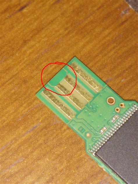
4. Connector and Mechanical Issues
USB connectors undergo frequent mating and unmating cycles, which can lead to mechanical stress and damage. Poorly designed or manufactured connectors can result in unreliable connections and device failures.
Solutions:
- Select high-quality USB connectors with robust mechanical design and durability.
- Ensure proper connector placement and alignment on the PCB.
- Use strain relief mechanisms to minimize mechanical stress on the connectors.
- Follow the manufacturer’s guidelines for connector soldering and assembly.
5. Compatibility and Interoperability
USB devices must be compatible with various USB hosts and comply with the USB standard’s specifications. Compatibility issues can arise due to differences in USB versions, protocols, or vendor-specific implementations.
Solutions:
- Thoroughly test the USB device with different USB hosts and operating systems.
- Implement proper USB enumeration and descriptor handling.
- Follow the USB standard’s guidelines for device classes and protocols.
- Consider using USB compliance testing tools and services to ensure interoperability.

USB PCB Design Considerations
To mitigate the problems mentioned above and ensure a robust USB PCB design, consider the following design considerations:
1. Layer Stack-up
- Use a multi-layer PCB with dedicated power and ground planes.
- Arrange the layers to minimize crosstalk and provide optimal signal routing.
- Consider using a 4-layer or 6-Layer PCB for better signal integrity and noise reduction.
2. Component Selection
- Choose USB controllers and transceivers that are compatible with the desired USB version and speed.
- Use high-quality passive components (resistors, capacitors) with tight tolerances.
- Select voltage regulators and power management ICs based on the power requirements of the USB device.
3. Signal Routing
- Route USB differential pairs with controlled impedance and length matching.
- Minimize the use of vias and layer transitions for high-speed signals.
- Keep USB traces away from noise sources and other high-speed signals.
4. Grounding and Shielding
- Implement a solid ground plane and use ground stitching vias to provide a low-impedance return path.
- Use ground fills or copper pours to minimize ground loops and improve shielding.
- Consider using shielded USB connectors or adding shielding components to the PCB.
5. Testing and Validation
- Perform signal integrity simulations and analyses to verify the USB PCB design.
- Conduct thorough testing of the USB device, including functional, performance, and compliance tests.
- Use USB protocol analyzers and oscilloscopes to debug and troubleshoot any issues.

USB PCB Manufacturing Considerations
In addition to the design considerations, pay attention to the manufacturing aspects of USB PCBs:
1. PCB Fabrication
- Choose a reputable PCB manufacturer with experience in high-speed PCB fabrication.
- Specify the correct PCB material, copper weight, and surface finish based on the USB requirements.
- Provide clear and comprehensive fabrication files, including Gerber files, drill files, and assembly drawings.
2. Assembly and Soldering
- Use appropriate soldering techniques for USB connectors and components, such as reflow soldering or wave soldering.
- Follow the manufacturer’s guidelines for solder paste application and component placement.
- Implement proper ESD (Electrostatic Discharge) protection measures during assembly.
3. Quality Control
- Perform visual inspections and automated optical inspections (AOI) to detect any manufacturing defects.
- Conduct electrical tests, such as continuity tests and boundary scan tests, to verify the integrity of the assembled PCB.
- Implement a robust quality control process to ensure consistent and reliable USB PCB manufacturing.

Frequently Asked Questions (FAQ)
1. What are the common USB versions and their data transfer speeds?
USB has evolved over the years, with different versions offering varying data transfer speeds:
– USB 1.1: Up to 12 Mbps (Full Speed)
– USB 2.0: Up to 480 Mbps (High Speed)
– USB 3.0: Up to 5 Gbps (SuperSpeed)
– USB 3.1: Up to 10 Gbps (SuperSpeed+)
– USB 3.2: Up to 20 Gbps (SuperSpeed+ 20Gbps)
2. What is the difference between USB Type-A, Type-B, and Type-C connectors?
- USB Type-A: The most common USB connector, found on host devices like computers and laptops.
- USB Type-B: Used on peripheral devices, such as printers and external hard drives.
- USB Type-C: A reversible connector that supports high-speed data transfer and power delivery. It is becoming increasingly popular in modern devices.
3. How can I ensure my USB device is compliant with the USB standard?
To ensure USB compliance, follow these steps:
– Refer to the USB Implementers Forum (USB-IF) specifications and guidelines.
– Use USB-IF certified components and controllers.
– Perform thorough testing, including compliance tests, using USB test tools and analyzers.
– Consider submitting your device for USB-IF certification.
4. What are the power requirements for different USB devices?
The power requirements for USB devices vary based on the USB version and device class:
– USB 2.0: Up to 500 mA at 5V (2.5 W)
– USB 3.0: Up to 900 mA at 5V (4.5 W)
– USB BC 1.2 (Battery Charging): Up to 1.5 A at 5V (7.5 W)
– USB Type-C: Up to 5A at 20V (100 W) with USB Power Delivery (USB PD)
5. How can I troubleshoot USB communication issues?
When encountering USB communication issues, try the following:
– Check the USB cable and connectors for any physical damage or loose connections.
– Verify that the USB device is properly enumerated and recognized by the host system.
– Use USB protocol analyzers or oscilloscopes to capture and analyze the USB traffic.
– Review the USB device firmware and driver implementation for any bugs or incompatibilities.
– Consult the USB device documentation and support resources for specific troubleshooting steps.
Conclusion
Designing and manufacturing USB PCBs can present various challenges, ranging from signal integrity issues to power management and compatibility concerns. By understanding these common problems and implementing appropriate solutions, you can overcome the obstacles and create reliable and high-performance USB devices.
Remember to follow best practices in USB PCB design, such as proper signal routing, grounding, and shielding techniques. Pay attention to the manufacturing considerations, including PCB fabrication, assembly, and quality control processes.
By addressing these problems and adhering to the USB standard’s guidelines, you can develop USB PCBs that meet the requirements of your specific application and provide a seamless user experience.
| USB Version | Data Transfer Speed |
|---|---|
| USB 1.1 | Up to 12 Mbps |
| USB 2.0 | Up to 480 Mbps |
| USB 3.0 | Up to 5 Gbps |
| USB 3.1 | Up to 10 Gbps |
| USB 3.2 | Up to 20 Gbps |
| USB Connector Type | Description |
|---|---|
| USB Type-A | Most common USB connector, found on host devices |
| USB Type-B | Used on peripheral devices, such as printers and external HDDs |
| USB Type-C | Reversible connector supporting high-speed data and power |
As USB technology continues to evolve, staying updated with the latest specifications, design techniques, and manufacturing processes is crucial. By keeping abreast of the advancements in USB PCB design and addressing the challenges head-on, you can create USB devices that are robust, reliable, and meet the ever-increasing demands of the market.


Leave a Reply