Introduction to USB PCB
A USB PCB (Printed Circuit Board) is the foundation of any device that utilizes a serial USB interface for communication and power transfer. USB, which stands for Universal Serial Bus, has become the standard protocol for connecting peripheral devices to computers and other electronic systems. The USB PCB plays a crucial role in ensuring reliable and efficient data transfer between the host and the connected device.
What is a USB PCB?
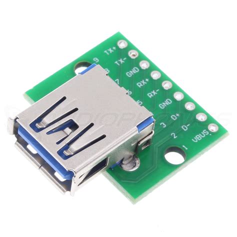
A USB PCB is a custom-designed circuit board that incorporates the necessary components and circuitry to enable USB communication. It typically includes a USB connector, a microcontroller or USB-to-serial converter chip, and various passive components such as resistors, capacitors, and inductors. The PCB layout is carefully designed to meet the stringent electrical requirements of the USB specification, ensuring signal integrity and minimizing electromagnetic interference (EMI).
Importance of USB PCB in USB Devices
The USB PCB is the core component of any USB device, as it handles the following critical functions:
1. USB Protocol Implementation: The PCB incorporates a microcontroller or dedicated USB-to-serial converter chip that implements the USB protocol stack. This enables the device to communicate with the host computer using the USB standard.
2. Power Management: USB PCBs often include power management circuitry to regulate the 5V supply provided by the USB port. This ensures that the connected device receives a stable and filtered power supply, preventing damage to sensitive components.
3. Signal Conditioning: The PCB layout is optimized to maintain signal integrity, minimizing crosstalk, reflections, and other signal degradation issues. Proper impedance matching and termination techniques are employed to ensure reliable data transmission.
4. ESD Protection: USB PCBs incorporate electrostatic discharge (ESD) protection measures to safeguard the device from potential damage caused by static electricity. This is particularly important for devices that are frequently plugged and unplugged.
USB PCB Design Considerations
Choosing the Right Components
When designing a USB PCB, selecting the appropriate components is crucial for optimal performance and reliability. The key components include:
1. USB Connector: The choice of USB connector depends on the device’s form factor and the intended USB version (USB 2.0, USB 3.0, etc.). Common options include USB Type-A, Type-B, Mini-USB, and Micro-USB connectors.
2. Microcontroller or USB-to-Serial Converter: The microcontroller or USB-to-serial converter chip is responsible for implementing the USB protocol and handling data transfer. Popular options include the FTDI FT232 series, Silicon Labs CP2102, and Microchip PIC18F series microcontrollers.
3. Passive Components: Resistors, capacitors, and inductors are used for various purposes, such as pull-up/pull-down resistors, decoupling capacitors, and ferrite beads for EMI suppression.
PCB Layout Guidelines
Proper PCB layout is essential for ensuring signal integrity and minimizing EMI. Some key guidelines for USB PCB layout include:
1. Impedance Matching: USB differential data lines (D+ and D-) should be routed as a differential pair with controlled impedance (usually 90Ω for USB 2.0 and 90Ω for USB 3.0).
2. Length Matching: The lengths of the D+ and D- traces should be matched to within a few millimeters to minimize skew and maintain signal integrity.
3. Ground Plane: A solid ground plane should be used to provide a low-impedance return path for the USB signals and to minimize EMI.
4. Decoupling Capacitors: Decoupling capacitors should be placed close to the power pins of the USB controller or converter chip to minimize power supply noise.
5. ESD Protection: ESD protection components, such as transient voltage suppressors (TVS) or varistors, should be placed near the USB connector to protect against electrostatic discharge.
USB PCB Fabrication and Assembly
Once the USB PCB design is finalized, it undergoes fabrication and assembly. The fabrication process involves the following steps:
1. PCB Manufacturing: The PCB design files are sent to a PCB manufacturer, who creates the physical board using a multi-layer fabrication process. This involves applying copper layers, insulating layers, and solder mask to the substrate material.
2. Component Procurement: The required components, such as the USB connector, microcontroller, and passive components, are sourced from reliable suppliers.
3. PCB Assembly: The components are soldered onto the fabricated PCB using either through-hole or surface-mount technology (SMT). Automated pick-and-place machines are commonly used for SMT assembly, ensuring precise component placement.
4. Testing and Quality Control: The assembled USB PCB undergoes rigorous testing to ensure functionality, signal integrity, and compliance with USB standards. This may include in-circuit testing, functional testing, and EMI testing.

USB PCB Applications and Examples
USB to Serial Converter
One of the most common applications of USB PCBs is in USB to serial converters. These devices allow legacy serial devices, such as modems, printers, and industrial equipment, to communicate with modern computers via USB. The USB PCB in these converters typically features a USB-to-serial converter chip, such as the FTDI FT232 or Silicon Labs CP2102, which handles the USB protocol and converts the data to serial format.
USB Flash Drives
USB flash drives, also known as thumb drives or pen drives, rely on USB PCBs for their functionality. The PCB in a USB flash drive includes a USB connector, a flash memory controller, and NAND flash memory chips. The memory controller manages the storage and retrieval of data, while the USB connector and circuitry enable communication with the host computer.
USB Hubs
USB hubs expand the number of available USB ports on a computer or device. The USB PCB in a hub includes a USB hub controller chip, which manages the communication between the upstream port (connected to the host) and the downstream ports (connected to the devices). The PCB also incorporates power management circuitry to ensure that each downstream port receives sufficient power.
USB Audio Interfaces
USB audio interfaces allow musicians and audio professionals to connect microphones, instruments, and other audio equipment to a computer for recording and playback. The USB PCB in these devices includes audio codecs, pre-amplifiers, and digital signal processing (DSP) chips to convert analog audio signals to digital data and vice versa. The PCB layout is optimized for low-noise performance and high-quality audio reproduction.

Frequently Asked Questions (FAQ)
-
What is the difference between USB 2.0 and USB 3.0 PCBs?
USB 3.0 PCBs are designed to support higher data transfer speeds (up to 5 Gbps) compared to USB 2.0 (up to 480 Mbps). USB 3.0 PCBs require additional differential pairs for the SuperSpeed data lines and have stricter layout requirements to maintain signal integrity at higher frequencies. -
Can a USB PCB be powered from the USB port itself?
Yes, a USB PCB can be powered directly from the USB port. The USB specification provides a 5V power supply with a maximum current of 500mA for USB 2.0 and 900mA for USB 3.0. However, if the device requires more power, an external power supply may be necessary. -
What are the common challenges in USB PCB design?
Some common challenges in USB PCB design include maintaining signal integrity, minimizing EMI, ensuring proper impedance matching, and adhering to the USB specification’s electrical requirements. Careful component selection, PCB layout, and testing are essential to overcome these challenges. -
How can I ensure my USB PCB is compliant with USB standards?
To ensure compliance with USB standards, it is important to follow the USB specification guidelines, use certified USB components, and adhere to best practices for PCB layout and design. Additionally, performing comprehensive testing, including compliance testing, can help validate the USB PCB’s conformance to the standards. -
Can I design a USB PCB with multiple USB ports?
Yes, a USB PCB can be designed with multiple USB ports. This is commonly seen in USB hubs, where a single upstream port is connected to multiple downstream ports. The PCB design must ensure proper power distribution, signal integrity, and compliance with the USB specification for each port.

Conclusion
USB PCBs are the backbone of any device that utilizes USB for communication and power. They play a crucial role in implementing the USB protocol, managing power, ensuring signal integrity, and providing ESD protection. When designing a USB PCB, careful consideration must be given to component selection, PCB layout, and adherence to USB standards. By following best practices and conducting thorough testing, engineers can create reliable and efficient USB devices that seamlessly integrate with a wide range of computing systems. As USB technology continues to evolve, USB PCBs will remain an essential component in enabling faster data transfer rates, improved power delivery, and enhanced functionality in a vast array of applications.


Leave a Reply