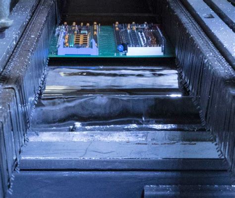
Understanding Solder Escape and Its Causes
Solder escape, also known as solder wicking, is a common issue faced during the reflow soldering process in PCB Assembly. It occurs when molten solder flows or “escapes” away from the intended solder joint, often along the component leads or PCB traces. This unwanted solder flow can lead to bridging, short circuits, and poor solder joint formation, compromising the reliability and functionality of the assembled PCB.
Several factors contribute to solder escape during reflow:
- Excessive solder paste application
- Improper solder paste viscosity
- Inadequate stencil design
- Incorrect reflow temperature profile
- Poor component placement accuracy
- Inappropriate PCB pad design
By understanding these causes, PCB manufacturers and assemblers can take proactive measures to minimize the occurrence of solder escape and ensure high-quality solder joints.
Optimizing Solder Paste Application
Proper solder paste application is crucial in preventing solder escape. Excessive solder paste can lead to solder bridging and wicking, while insufficient paste may result in weak solder joints. Here are some tips to optimize solder paste application:
Stencil Design
- Use a stencil thickness appropriate for the component pitch and lead size. A general guideline is to use a stencil thickness that is 80-90% of the lead diameter.
- Ensure proper aperture dimensions and shape based on the pad size and component type. Consult the component manufacturer’s recommendations for optimal aperture design.
- Incorporate aperture reduction for fine-pitch components to control solder paste volume.
- Use step stencils or multi-level stencils for PCBs with varying component heights to ensure consistent paste deposition.
| Component Pitch | Recommended Stencil Thickness |
|---|---|
| > 0.65 mm | 150 – 200 μm |
| 0.5 – 0.65 mm | 120 – 150 μm |
| 0.4 – 0.5 mm | 100 – 120 μm |
| < 0.4 mm | 80 – 100 μm |
Solder Paste Printing
- Maintain proper printer alignment and calibration to ensure accurate paste deposition.
- Use a suitable squeegee blade material (e.g., metal or polyurethane) and maintain the blade in good condition.
- Optimize squeegee pressure, speed, and angle to achieve consistent paste deposition across the stencil.
- Regularly clean the stencil to prevent paste buildup and contamination.
- Monitor paste viscosity and replace the paste as needed to maintain consistent print quality.

Controlling Solder Paste Viscosity
Solder paste viscosity plays a significant role in preventing solder escape. The ideal viscosity allows the paste to flow and form a proper solder joint without excessive spreading or wicking. Here are some tips to control solder paste viscosity:
- Select a solder paste with the appropriate viscosity for your application. Consult the paste manufacturer’s recommendations based on the component types and PCB design.
- Store solder paste at the recommended temperature (typically 0-10°C) to maintain its shelf life and viscosity stability.
- Allow the paste to reach room temperature before use to ensure optimal viscosity for printing.
- Regularly monitor the paste’s viscosity using a viscometer or flow testing methods.
- Adjust the reflow profile, particularly the soak zone, to allow the paste to reach the desired viscosity before entering the reflow zone.
| Solder Paste Type | Viscosity Range (Pa·s) | Suitable Applications |
|---|---|---|
| Type 3 | 800 – 1200 | General purpose, standard components |
| Type 4 | 600 – 1000 | Fine-pitch components, SMD devices |
| Type 5 | 400 – 800 | Ultra-fine pitch, micron-scale parts |

Reflow Profile Optimization
The reflow temperature profile significantly influences solder escape. An incorrect profile can cause excessive solder flow, leading to wicking and bridging. Here are some guidelines for optimizing the reflow profile:
- Follow the solder paste manufacturer’s recommended reflow profile as a starting point.
- Use a multi-stage reflow profile with distinct preheat, soak, reflow, and cooling zones.
- Set the peak reflow temperature based on the solder paste specifications and PCB/component limitations. Typically, it should be 20-30°C above the solder alloy’s melting point.
- Control the ramp-up rate during preheating to allow gradual and uniform temperature increase across the PCB.
- Adjust the soak zone duration and temperature to achieve proper paste activation and avoid thermal shock to components.
- Minimize the time above liquidus (TAL) to prevent excessive solder flow and intermetallic growth.
- Ensure proper cooling rate to facilitate solder joint solidification and prevent thermal stress.
| Reflow Zone | Temperature Range | Duration |
|---|---|---|
| Preheat | 150 – 180°C | 60 – 120s |
| Soak | 180 – 200°C | 60 – 120s |
| Reflow | 230 – 250°C | 30 – 60s |
| Cooling | < 100°C | < 90s |

Enhancing Component Placement Accuracy
Accurate component placement is essential for preventing solder escape. Misaligned or shifted components can cause solder bridging and wicking. Follow these tips to improve component placement accuracy:
- Use a high-quality pick-and-place machine with proper calibration and alignment.
- Ensure accurate fiducial recognition and placement offset correction.
- Implement vision systems to verify component placement before reflow.
- Use appropriate nozzle sizes and shapes for different component types.
- Maintain proper component feeder setup and tape/reel alignment.
- Regularly clean the nozzles and replace worn or damaged ones.
- Optimize placement force and speed based on component size and fragility.
PCB Pad Design Considerations
PCB pad design plays a crucial role in preventing solder escape. Proper pad dimensions, spacing, and solder mask openings can help confine the solder flow and prevent wicking. Consider the following pad design tips:
- Follow the component manufacturer’s recommended pad dimensions for optimal solder joint formation.
- Maintain sufficient pad-to-pad spacing to prevent solder bridging, especially for fine-pitch components.
- Use solder mask-defined (SMD) pads to constrain solder flow and prevent bridging.
- Ensure proper solder mask expansion and registration to avoid exposed copper areas that can cause solder wicking.
- Implement teardrops or fillets at pad-to-trace transitions to strengthen the solder joint and reduce stress concentration.
| Component Type | Pad Width (mm) | Pad Length (mm) | Pad Spacing (mm) |
|---|---|---|---|
| 0805 | 0.5 – 0.7 | 1.0 – 1.4 | 0.5 – 0.8 |
| 0603 | 0.3 – 0.5 | 0.8 – 1.0 | 0.3 – 0.5 |
| 0402 | 0.2 – 0.3 | 0.5 – 0.7 | 0.2 – 0.3 |
| 0201 | 0.15 – 0.25 | 0.3 – 0.4 | 0.15 – 0.25 |
Frequently Asked Questions (FAQ)
-
Q: What are the most common causes of solder escape during reflow?
A: The most common causes of solder escape include excessive solder paste application, incorrect solder paste viscosity, improper stencil design, non-optimal reflow temperature profile, poor component placement accuracy, and inappropriate PCB pad design. -
Q: How can I optimize my solder paste printing process to prevent solder escape?
A: To optimize solder paste printing, use a stencil with the appropriate thickness and aperture dimensions, maintain proper printer alignment and calibration, use a suitable squeegee blade, optimize squeegee pressure and speed, regularly clean the stencil, and monitor paste viscosity. -
Q: What is the ideal solder paste viscosity for preventing solder escape?
A: The ideal solder paste viscosity depends on the specific application and component types. Generally, Type 3 paste (800-1200 Pa·s) is suitable for general-purpose and standard components, while Type 4 paste (600-1000 Pa·s) is recommended for fine-pitch components and SMD devices. -
Q: How can I optimize my reflow profile to minimize solder escape?
A: To optimize the reflow profile, follow the solder paste manufacturer’s recommendations, use a multi-stage profile with distinct zones (preheat, soak, reflow, cooling), set the peak reflow temperature based on the solder alloy’s melting point, control the ramp-up rate, adjust the soak zone duration, minimize time above liquidus, and ensure proper cooling rate. -
Q: What PCB pad design considerations help prevent solder escape?
A: To prevent solder escape through pad design, follow the component manufacturer’s recommended pad dimensions, maintain sufficient pad-to-pad spacing, use solder mask-defined (SMD) pads, ensure proper solder mask expansion and registration, and implement teardrops or fillets at pad-to-trace transitions.
By implementing these tips and tricks across various aspects of the PCB assembly process, manufacturers and assemblers can significantly reduce the occurrence of solder escape and improve the overall quality and reliability of their solder joints during reflow soldering.


Leave a Reply