Introduction to PCB Silkscreening
Printed circuit boards (PCBs) are essential components in virtually all modern electronic devices. These boards provide the foundation upon which various electronic components are mounted and interconnected to create functional circuits. One critical aspect of PCB manufacturing is the application of informative markings and labels on the board’s surface, a process known as PCB silkscreening.
Silkscreening, also referred to as screen printing, is a versatile printing technique that has found extensive use in the PCB industry. This method involves transferring ink through a fine mesh screen onto the surface of the PCB, creating clear and durable markings that serve multiple purposes. In this article, we will delve into the intricacies of PCB silkscreening, exploring its importance, the process involved, and best practices for achieving optimal results.
The Importance of PCB Silkscreening
PCB silkscreening plays a vital role in the manufacturing and assembly of electronic devices. The markings and labels applied through this process serve several essential functions:
-
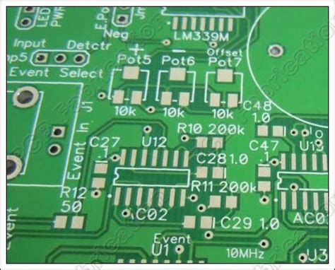
Component Identification: Silkscreened markings help identify the location and orientation of electronic components on the PCB. This information is crucial for accurate assembly and troubleshooting.
-
Reference Designators: Each component on a PCB is assigned a unique reference designator, such as R1 for a resistor or C2 for a capacitor. Silkscreening these designators next to the corresponding components facilitates easy identification and referencing.
-
Polarity Indicators: Some components, such as electrolytic capacitors and diodes, have specific polarity requirements. Silkscreened polarity indicators, like plus (+) and minus (-) signs, ensure correct Component Orientation during assembly.
-
Test Points: Silkscreened test points provide designated locations for probing and testing the PCB during validation and debugging processes.
-
Branding and Aesthetics: Silkscreening allows for the inclusion of company logos, product names, and other branding elements on the PCB. This enhances the professional appearance of the final product.

The PCB Silkscreening Process
The PCB silkscreening process involves several steps to achieve precise and durable markings on the board’s surface. Here’s a breakdown of the process:
Step 1: Screen Preparation
The first step in PCB silkscreening is the creation of the screen, also known as the stencil. The screen is typically made of a fine mesh material, such as polyester or stainless steel, stretched tightly over a frame. The desired artwork, containing the markings and labels to be printed, is transferred onto the screen using a photosensitive emulsion.
Step 2: Ink Application
Once the screen is prepared, it is placed over the PCB, and ink is applied to the top of the screen. The ink used in PCB silkscreening is specially formulated to adhere to the board’s surface and withstand the rigors of the manufacturing process. The most common ink colors are white and yellow, as they provide good contrast against the typical green solder mask used on PCBs.
Step 3: Printing
With the ink in place, a squeegee is used to force the ink through the openings in the screen and onto the surface of the PCB. The squeegee is moved across the screen in a controlled manner, ensuring even distribution of the ink and consistent coverage of the artwork.
Step 4: Curing
After printing, the ink needs to be cured to ensure its durability and adhesion to the PCB surface. Curing is typically done using heat, either through oven baking or exposure to ultraviolet (UV) light. The curing process helps the ink to solidify and become resistant to abrasion and chemicals.
Step 5: Inspection
The final step in the PCB silkscreening process is inspection. The printed PCBs are carefully examined to ensure the accuracy, legibility, and proper alignment of the silkscreened markings. Any defects or inconsistencies are identified and corrected before the PCBs move on to the next stage of manufacturing.

Best Practices for PCB Silkscreening
To achieve the best results in PCB silkscreening, consider the following best practices:
-
Artwork Design: Ensure that the artwork for silkscreening is designed with clarity and readability in mind. Use appropriate font sizes, line widths, and spacing to guarantee legibility.
-
Ink Selection: Choose high-quality inks that are specifically formulated for PCB silkscreening. Consider factors such as durability, adhesion, and compatibility with the PCB Surface Finish.
-
Screen Tension: Maintain proper screen tension to ensure consistent ink deposition and prevent distortion of the printed artwork.
-
Squeegee Pressure and Angle: Apply appropriate squeegee pressure and maintain a consistent angle during the printing process to achieve even ink distribution and avoid smudging.
-
Curing Parameters: Follow the recommended curing parameters, such as temperature and duration, to ensure optimal ink adhesion and durability.

Advantages of PCB Silkscreening
PCB silkscreening offers several advantages over other marking methods:
-
Durability: Silkscreened markings are highly durable and resistant to abrasion, chemicals, and environmental factors, ensuring long-lasting legibility.
-
Precision: The silkscreening process allows for precise and detailed markings, enabling the inclusion of intricate artwork and small text.
-
Efficiency: Silkscreening is a fast and efficient process, making it suitable for high-volume PCB production.
-
Cost-effectiveness: Compared to other marking methods, such as direct printing or labeling, silkscreening is a cost-effective solution for applying markings to PCBs.
Challenges and Considerations
While PCB silkscreening is a widely used and reliable process, there are some challenges and considerations to keep in mind:
-
Compatibility with Surface Finishes: Certain surface finishes, such as hard gold or silver, may not provide optimal adhesion for silkscreened inks. It’s important to select compatible inks and test for adhesion before mass production.
-
Miniaturization: As PCBs become increasingly miniaturized, the available space for silkscreened markings decreases. This requires careful artwork design and precise printing to ensure legibility.
-
Color Limitations: While white and yellow are the most common colors used in PCB silkscreening, achieving other colors may require specialized inks and processes.
-
Artwork Revisions: Making changes to the silkscreened artwork can be time-consuming and costly, as it requires the creation of new screens. Thorough review and approval of the artwork before production are crucial.
Frequently Asked Questions (FAQ)
1. What is the purpose of silkscreening on PCBs?
A: PCB silkscreening serves multiple purposes, including component identification, reference designator marking, polarity indication, test point designation, and branding. These markings help in the assembly, testing, and troubleshooting of electronic devices.
2. Can silkscreening be applied to both sides of a PCB?
A: Yes, silkscreening can be applied to both the top and bottom sides of a PCB. However, it’s important to consider the placement of components and ensure that the silkscreened markings do not interfere with their functionality.
3. How durable are silkscreened markings on PCBs?
A: Silkscreened markings are highly durable and resistant to abrasion, chemicals, and environmental factors. With proper ink selection and curing, these markings can withstand the rigors of the manufacturing process and maintain legibility throughout the life of the PCB.
4. Can silkscreening be used on Flexible PCBs?
A: Yes, silkscreening can be applied to flexible PCBs. However, the ink and curing process may need to be adjusted to accommodate the flexible substrate and ensure proper adhesion and durability.
5. Are there any limitations to the level of detail that can be achieved with silkscreening?
A: While silkscreening allows for precise and detailed markings, there are limitations based on factors such as screen mesh size, ink viscosity, and artwork design. Very fine details or extremely small text may be challenging to reproduce consistently. It’s important to work with experienced PCB manufacturers and discuss the feasibility of specific artwork requirements.
Conclusion
PCB silkscreening is a crucial process in the manufacturing of printed circuit boards, providing essential markings and labels that aid in assembly, testing, and identification. By understanding the importance of silkscreening, the process involved, and best practices, PCB designers and manufacturers can ensure the creation of high-quality and functional boards.
As the electronics industry continues to evolve, with increasing miniaturization and complexity, the role of PCB silkscreening remains significant. Advancements in materials, processes, and equipment will further enhance the capabilities and efficiency of this vital technique.
By leveraging the power of PCB silkscreening and following industry best practices, manufacturers can produce PCBs that not only meet functional requirements but also showcase clear and informative markings that contribute to the overall quality and usability of electronic devices.
| Aspect | Description |
|---|---|
| Purpose | Component identification, reference designators, polarity indication, test points, branding |
| Process Steps | Screen preparation, ink application, printing, curing, inspection |
| Ink Colors | Commonly white and yellow for good contrast against green solder mask |
| Advantages | Durability, precision, efficiency, cost-effectiveness |
| Challenges | Compatibility with surface finishes, miniaturization, color limitations, artwork revisions |
Table 1: Key aspects of PCB silkscreening.
In summary, PCB silkscreening is an indispensable process in the realm of printed circuit board manufacturing. Its ability to provide clear, durable, and informative markings on the surface of PCBs contributes significantly to the functionality, assembly, and maintenance of electronic devices. By understanding and implementing best practices in PCB silkscreening, manufacturers can ensure the production of high-quality boards that meet the ever-evolving demands of the electronics industry.


Leave a Reply