What is PCB Silkscreen?
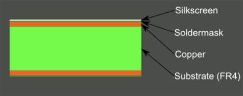
PCB silkscreen, also known as legend or nomenclature, is a layer of text and symbols printed on the surface of a printed circuit board (PCB) to provide essential information for assembly, testing, and maintenance. The silkscreen layer is typically white, although other colors like yellow or black can be used for better contrast or aesthetic purposes. The silkscreen is usually applied on the component side of the PCB, but can also be found on the solder side in some cases.
Purpose of PCB Silkscreen
The main purposes of PCB silkscreen are:
-
Component identification: Silkscreen labels components with their reference designators (e.g., R1, C2, U3) and values (e.g., 10K, 100nF, 74HC00), making it easier for technicians to locate and identify them during assembly and troubleshooting.
-
Orientation markers: Silkscreen provides orientation markers, such as pin 1 indicators and polarity signs, to ensure correct placement and orientation of components.
-
Test points and fiducials: Silkscreen can mark test points and fiducials, which are used for automated optical inspection (AOI) and pick-and-place machines.
-
Branding and logos: Silkscreen can include company logos, product names, and revision numbers for branding and version control purposes.
-
Warning and safety information: Silkscreen can display warning symbols and safety instructions to prevent misuse or damage to the PCB.
Silkscreen Design Guidelines
To ensure readability and clarity of the silkscreen, follow these design guidelines:
-
Font size: Use a minimum font size of 0.8mm (0.032″) for text and 0.6mm (0.024″) for subscript characters. Larger fonts are preferable for better legibility.
-
Line width: Use a minimum line width of 0.15mm (0.006″) for silkscreen graphics and text outlines.
-
Clearance: Maintain a minimum clearance of 0.15mm (0.006″) between silkscreen and exposed copper, solder mask openings, and board edges to prevent shorting and manufacturing issues.
-
Contrast: Ensure adequate contrast between the silkscreen color and the background (usually solder mask) for optimal readability.
-
Placement: Avoid placing silkscreen over component pads, vias, or other critical features that may interfere with soldering or inspection.
PCB Silkscreen Application Methods
There are two primary methods for applying silkscreen to PCBs:
1. Screen Printing
Screen printing is the traditional and most common method for applying silkscreen to PCBs. The process involves the following steps:
-
A fine mesh screen is coated with a light-sensitive emulsion and exposed to UV light through a film positive of the silkscreen artwork.
-
The unexposed areas of the emulsion are washed away, leaving a stencil of the silkscreen design on the mesh.
-
The screen is placed over the PCB, and ink is forced through the mesh onto the board using a squeegee.
-
The ink is then cured using heat or UV light to form a permanent layer on the PCB surface.
Screen printing is suitable for high-volume production and can produce durable, high-quality silkscreen layers.
2. Direct Legend Printing (DLP)
Direct legend printing is a digital printing method that uses inkjet or laser technology to apply the silkscreen directly onto the PCB surface. The process involves the following steps:
-
The silkscreen artwork is loaded into the DLP machine’s software.
-
The PCB is placed in the machine, and the silkscreen ink is applied directly onto the board using inkjet or laser printheads.
-
The ink is cured using heat or UV light to form a permanent layer on the PCB surface.
DLP is suitable for low-volume production, prototyping, and quick turnaround times. It offers more flexibility in terms of customization and design changes compared to screen printing.

PCB Silkscreen Ink Curing Methods
After applying the silkscreen ink to the PCB, it must be cured to form a permanent, durable layer. There are two main curing methods:
1. Thermal Curing
Thermal curing involves exposing the printed PCB to heat in an oven or on a conveyor belt. The temperature and duration of the curing process depend on the type of ink and the PCB material. Typical curing temperatures range from 120°C to 150°C (248°F to 302°F), with curing times of 10 to 30 minutes.
Advantages of thermal curing:
– Suitable for most ink types and PCB materials
– Produces a durable, scratch-resistant silkscreen layer
– Can be used for high-volume production
Disadvantages of thermal curing:
– Slower process compared to UV curing
– Requires more energy and space for the curing equipment
– May cause warping or damage to heat-sensitive components
2. UV Curing
UV curing involves exposing the printed PCB to high-intensity ultraviolet light to polymerize the ink. The process is much faster than thermal curing, typically taking only a few seconds to a minute. UV-curable inks contain photoinitiators that react with the UV light to form a solid, durable layer.
Advantages of UV curing:
– Fast curing process, suitable for high-volume production
– Lower energy consumption compared to thermal curing
– Minimal heat exposure, reducing the risk of damaging heat-sensitive components
Disadvantages of UV curing:
– Requires special UV-curable inks, which may be more expensive than regular inks
– May not be suitable for all PCB materials, as some may not be UV-transparent
– Requires additional safety measures to protect operators from UV exposure

FAQ
1. Can silkscreen be applied to both sides of a PCB?
Yes, silkscreen can be applied to both the component side and the solder side of a PCB. However, it is more common to have silkscreen on the component side only, as it provides the most relevant information for assembly and troubleshooting.
2. Is it possible to have multi-colored silkscreen on a PCB?
Yes, it is possible to have multi-colored silkscreen on a PCB, although it is less common than single-color silkscreen. Multi-colored silkscreen requires additional printing steps and may increase the cost of the PCB. It is typically used for aesthetic purposes or to convey more complex information.
3. Can silkscreen be removed or modified after the PCB is manufactured?
Removing or modifying silkscreen after the PCB is manufactured is difficult and not recommended. Silkscreen is designed to be a permanent layer, and attempting to remove it may damage the PCB or other components. If changes to the silkscreen are necessary, it is best to revise the artwork and manufacture new PCBs.
4. How does the choice of solder mask color affect the visibility of the silkscreen?
The choice of solder mask color can significantly affect the visibility and readability of the silkscreen. White silkscreen on a dark-colored solder mask (e.g., green, blue, or black) provides the best contrast and readability. If a light-colored solder mask is used (e.g., red or yellow), a black or dark-colored silkscreen may be more appropriate for better visibility.
5. Can silkscreen be used on flexible or Rigid-Flex PCBs?
Yes, silkscreen can be applied to flexible and rigid-flex PCBs, although the process may require some modifications compared to rigid PCBs. The ink and curing method must be compatible with the flexible substrate material, and the design should account for the bending and flexing of the PCB to ensure the durability of the silkscreen layer.
In conclusion, PCB silkscreen is an essential element of PCB design and manufacturing, providing crucial information for assembly, testing, and maintenance. By following design guidelines and choosing the appropriate application and curing methods, PCB manufacturers can produce high-quality, durable silkscreen layers that enhance the functionality and usability of their products.


Leave a Reply