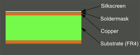
What is PCB Silkscreen?
PCB silkscreen, also known as legend or nomenclature, is the layer of text and symbols printed on the surface of a printed circuit board (PCB). The purpose of the silkscreen is to provide essential information about the components, their placement, and the overall functionality of the board. This information is crucial for assembling, testing, and debugging the PCB.
The silkscreen is typically printed using a white or yellow ink, although other colors may be used for specific applications. The ink is applied through a screen printing process, similar to how designs are printed on t-shirts.
Importance of PCB Silkscreen
PCB silkscreen serves several important functions:
-
Component Identification: The silkscreen labels each component on the board with its reference designator (e.g., R1, C2, U3), making it easier for technicians to identify and place components during assembly.
-
Orientation Indicators: Silkscreen markings often include orientation indicators for components such as diodes, electrolytic capacitors, and ICs, ensuring they are placed correctly on the board.
-
Test Points: The silkscreen may label test points, allowing technicians to quickly locate and probe specific points on the board during testing and debugging.
-
Branding and Logos: Silkscreen can be used to print company logos, product names, or other branding elements on the PCB.
-
Regulatory Information: Silkscreen may include regulatory information, such as certification marks (e.g., UL, CE, RoHS), to demonstrate compliance with industry standards.
Steps to Achieve Satisfied PCB Silkscreen
To ensure a high-quality and satisfactory PCB silkscreen, follow these steps:
Step 1: Design Preparation
-
Create a Separate Silkscreen Layer: In your PCB design software, create a dedicated layer for the silkscreen. This layer should be separate from the copper layers and the solder mask layer.
-
Use Vector Graphics: Design your silkscreen using vector graphics rather than raster images. Vector graphics can be scaled without losing quality and are easier to modify if needed.
-
Keep It Simple: Avoid overly complex designs or small, intricate details that may be difficult to print clearly on the PCB surface.
-
Maintain Clearance: Ensure that the silkscreen elements maintain sufficient clearance from the copper traces, pads, and other components to avoid interference or short circuits.
Step 2: Font Selection
-
Choose a Legible Font: Select a font that is easy to read, even at small sizes. Sans-serif fonts like Arial, Helvetica, or Verdana are often good choices.
-
Consider Font Size: Use a font size that is large enough to be easily readable but not so large that it takes up too much space on the PCB. A minimum font size of 0.8mm is generally recommended.
-
Consistent Font Usage: Use the same font throughout the silkscreen design for a cohesive and professional look.
Step 3: Text and Symbol Placement
-
Component Labeling: Place the reference designator for each component close to the component itself, ensuring that the label does not overlap with the component or its pads.
-
Orientation Indicators: Include orientation indicators for components that require specific placement, such as diodes and electrolytic capacitors. Use standard symbols like a small triangle or a dot to indicate the correct orientation.
-
Alignment: Align text and symbols neatly and consistently. Use grid lines or alignment tools in your PCB design software to ensure proper placement.
-
Polarity Marking: Clearly mark the polarity of components like diodes, LEDs, and electrolytic capacitors using the appropriate symbols (e.g., a plus sign for the positive terminal).
Step 4: Silkscreen Color Selection
-
Contrast: Choose a silkscreen color that contrasts well with the PCB substrate and the solder mask. White or yellow ink on a green solder mask is a common choice.
-
Consistency: Use the same silkscreen color throughout the design for a consistent appearance.
-
Special Requirements: If your PCB has specific color requirements (e.g., for color-coding or branding), ensure that the silkscreen color is appropriate and complies with any relevant standards.
Step 5: Design Review and Verification
-
Proofreading: Carefully proofread all text on the silkscreen layer to ensure accuracy and correct any spelling or grammatical errors.
-
Design Rule Check (DRC): Run a DRC on your PCB design software to check for any silkscreen-related issues, such as overlapping elements or insufficient clearance.
-
Manufacturing Constraints: Consult with your PCB manufacturer to ensure that your silkscreen design meets their specific manufacturing constraints, such as minimum line width and text size.
-
Prototype Testing: If possible, order a prototype of your PCB to verify the quality and legibility of the silkscreen. This will allow you to make any necessary adjustments before mass production.

FAQs
-
Q: Can silkscreen be applied to both sides of the PCB?
A: Yes, silkscreen can be applied to both the top and bottom sides of the PCB, depending on your design requirements. -
Q: Is it possible to have multiple colors in the silkscreen?
A: While it is possible to use multiple colors in the silkscreen, it is less common and may increase the cost of manufacturing. Most PCBs use a single color (usually white or yellow) for the silkscreen. -
Q: What is the minimum line width for PCB silkscreen?
A: The minimum line width for PCB silkscreen varies depending on the manufacturer but is typically around 0.15mm to 0.2mm. -
Q: Can I use silkscreen to print images or logos on the PCB?
A: Yes, you can use silkscreen to print images or logos on the PCB. However, keep in mind that intricate designs or small details may not print clearly. It’s best to consult with your PCB manufacturer for guidance on image printing. -
Q: Is there an additional cost for adding silkscreen to my PCB?
A: In most cases, adding silkscreen to your PCB does not incur a significant additional cost, as it is a standard part of the PCB manufacturing process. However, if you require multiple colors or have a particularly complex silkscreen design, there may be additional charges.

Conclusion
PCB silkscreen is a crucial element in the design and manufacture of printed circuit boards. By following the steps outlined in this guide, you can ensure that your PCB silkscreen is legible, informative, and aesthetically pleasing. Remember to keep your design simple, use appropriate fonts and colors, and maintain proper clearance between silkscreen elements and other components.
Always consult with your PCB manufacturer to ensure that your silkscreen design meets their specific manufacturing constraints and guidelines. By working closely with your manufacturer and following best practices for PCB silkscreen design, you can achieve a high-quality, professional-looking PCB that is easy to assemble, test, and debug.
| Silkscreen Element | Recommended Specification |
|---|---|
| Font | Sans-serif (e.g., Arial, Helvetica, Verdana) |
| Font Size | Minimum 0.8mm |
| Line Width | Minimum 0.15mm to 0.2mm |
| Clearance | Sufficient clearance from copper traces, pads, and components |
| Color | High contrast with PCB substrate and solder mask (e.g., white or yellow on green) |
By adhering to these recommended specifications and following the step-by-step guide provided, you can achieve a satisfied PCB silkscreen that enhances the overall quality and functionality of your printed circuit board.


Leave a Reply