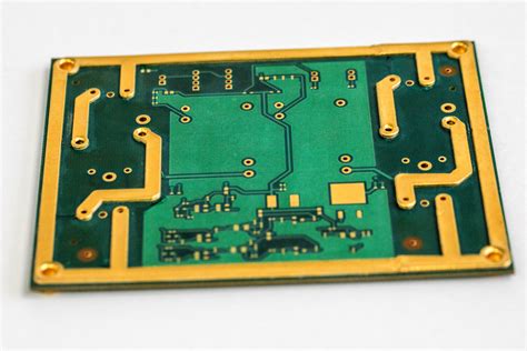
What are PCBs?
PCBs are flat boards made of insulating materials, such as fiberglass or plastic, with conductive pathways etched or printed onto the surface. These pathways, also known as traces, connect various electronic components, such as resistors, capacitors, and integrated circuits (ICs), to form a complete electronic circuit. PCBs provide a stable and compact platform for these components, enabling the efficient transfer of electrical signals and power.
History of PCBs
The concept of PCBs dates back to the early 20th century when Albert Hanson, a German inventor, filed a patent for a printed wire board in 1903. However, it wasn’t until the 1940s that PCBs began to gain widespread adoption. During World War II, the United States military heavily relied on PCBs for their electronic equipment, as they provided a more compact, reliable, and cost-effective solution compared to traditional point-to-point wiring.
In the 1950s and 1960s, PCBs underwent significant advancements, with the introduction of double-sided boards and through-hole technology. These developments allowed for more complex circuits and higher component density. The 1970s saw the emergence of multi-layer PCBs, which further increased circuit complexity and density by allowing for the stacking of multiple conductive layers.
The 1980s and 1990s brought about the widespread adoption of surface-mount technology (SMT), which revolutionized PCB manufacturing by enabling the placement of smaller components directly onto the board’s surface. This advancement led to even more compact and efficient PCB designs.

PCB Manufacturing Process
The PCB manufacturing process involves several key steps, each of which is crucial to ensuring the quality and reliability of the final product. These steps include:
-
Design: The PCB design process begins with the creation of a schematic diagram, which outlines the electronic circuit and its components. This schematic is then translated into a PCB layout, which defines the physical placement of components and the routing of conductive traces.
-
Printing: The PCB layout is used to create a photomask, which is a template for transferring the circuit pattern onto the PCB substrate. The substrate, typically made of fiberglass or plastic, is coated with a light-sensitive material called photoresist. The photomask is placed on top of the photoresist-coated substrate and exposed to UV light, hardening the exposed areas of the photoresist.
-
Etching: The unexposed areas of the photoresist are removed, revealing the bare substrate. The board is then placed in an etching solution, which removes the unwanted copper, leaving only the desired conductive traces.
-
Drilling: Holes are drilled into the PCB to accommodate through-hole components and provide interconnections between layers in multi-layer boards.
-
Plating: The drilled holes are plated with a conductive material, typically copper, to ensure proper electrical connectivity between layers.
-
Solder Mask Application: A protective solder mask is applied to the PCB surface, covering the areas where soldering is not required. This mask helps prevent short circuits and improves the board’s durability.
-
Silkscreen Printing: A silkscreen layer is printed onto the PCB, providing labels, logos, and other identifying information.
-
Surface Finish: A surface finish, such as HASL (Hot Air Solder Leveling), ENIG (Electroless Nickel Immersion Gold), or OSP (Organic Solderability Preservative), is applied to the exposed copper traces to prevent oxidation and enhance solderability.
-
Electrical Testing: The completed PCB undergoes electrical testing to ensure proper functionality and adherence to design specifications.

Types of PCBs
There are several types of PCBs, each designed to meet specific requirements and applications. The most common types include:
-
Single-Layer PCBs: These boards have conductive traces on only one side of the substrate. They are the simplest and most cost-effective type of PCB, suitable for basic electronic circuits.
-
Double-layer PCBs: These boards have conductive traces on both sides of the substrate, allowing for more complex circuits and higher component density compared to single-layer PCBs.
-
Multi-layer PCBs: These boards consist of multiple layers of conductive traces sandwiched between insulating layers. They offer the highest level of circuit complexity and density, making them ideal for advanced electronic applications.
-
Flexible PCBs: These boards are made of flexible materials, such as polyimide, allowing them to bend and conform to various shapes. They are commonly used in wearable electronics, medical devices, and aerospace applications.
-
Rigid-Flex PCBs: These boards combine the benefits of both rigid and flexible PCBs, featuring rigid sections for mounting components and flexible sections for interconnections. They are often used in applications requiring high reliability and space savings.

PCB Applications
PCBs are used in a wide range of electronic applications across various industries. Some of the most common applications include:
-
Consumer Electronics: PCBs are found in smartphones, tablets, laptops, televisions, gaming consoles, and home appliances.
-
Automotive Electronics: Modern vehicles heavily rely on PCBs for various systems, such as engine control units, infotainment systems, and advanced driver assistance systems (ADAS).
-
Medical Devices: PCBs are crucial components in medical equipment, including patient monitors, imaging systems, and implantable devices.
-
Industrial Automation: PCBs play a vital role in industrial control systems, such as programmable logic controllers (PLCs), sensors, and motor drives.
-
Aerospace and Defense: PCBs are used in a wide range of aerospace and defense applications, including avionics, satellite systems, and military communication equipment.
-
Telecommunications: PCBs are essential for telecommunications infrastructure, such as routers, switches, and base stations.
-
Internet of Things (IoT): The proliferation of IoT devices has driven the demand for compact, low-power PCBs that can enable wireless connectivity and sensor integration.
Future Trends in PCB Technology
As electronic devices continue to evolve and become more sophisticated, PCB technology must keep pace to meet the ever-increasing demands for performance, reliability, and miniaturization. Some of the key trends shaping the future of PCBs include:
-
High-Density Interconnect (HDI) PCBs: HDI PCBs feature finer traces, smaller vias, and higher component density, enabling the development of more compact and powerful electronic devices.
-
Embedded Components: The integration of passive components, such as resistors and capacitors, directly into the PCB substrate, reduces the overall footprint and improves signal integrity.
-
Advanced Materials: The use of advanced PCB materials, such as high-frequency laminates and low-loss dielectrics, enables the design of PCBs for high-speed and high-frequency applications, such as 5G networks and millimeter-wave radar.
-
3D Printing: The adoption of 3D printing technologies for PCB fabrication offers the potential for rapid prototyping, customization, and the creation of complex, non-planar PCB structures.
-
Environmental Sustainability: There is a growing emphasis on the development of eco-friendly PCB materials and manufacturing processes to reduce the environmental impact of electronic waste.
Frequently Asked Questions (FAQ)
-
What is the difference between a PCB and a printed wiring board (PWB)?
A PCB and a PWB are essentially the same things. The term “printed wiring board” was used in the early days of PCB development, but “printed circuit board” has become the more common term in recent years. -
How do I choose the right type of PCB for my project?
The choice of PCB type depends on several factors, including the complexity of the circuit, the required component density, the operating environment, and the budget. Single-layer and double-layer PCBs are suitable for simpler circuits, while multi-layer PCBs are ideal for more complex designs. Flexible and rigid-flex PCBs are used in applications requiring flexibility or space savings. -
What is the typical turnaround time for PCB manufacturing?
The turnaround time for PCB manufacturing varies depending on the complexity of the design, the chosen manufacturer, and the order quantity. Simple PCBs can be manufactured in as little as 24 hours, while more complex designs may take several weeks. It is essential to discuss lead times with your chosen PCB manufacturer to ensure your project stays on schedule. -
How can I ensure the quality and reliability of my PCBs?
To ensure the quality and reliability of your PCBs, it is crucial to work with a reputable PCB manufacturer that adheres to industry standards and quality control processes. Additionally, thorough design reviews, prototyping, and testing can help identify and address any potential issues before mass production. -
What is the cost of PCB manufacturing, and how can I optimize it?
The cost of PCB manufacturing depends on various factors, such as the board size, layer count, material choice, and order quantity. To optimize costs, consider designing for manufacturability (DFM), which involves adhering to your chosen manufacturer’s design guidelines and minimizing complexity where possible. Ordering larger quantities can also result in lower per-unit costs due to economies of scale.
Conclusion
PCBs are indispensable components in modern electronics, providing the foundation for the functionality and reliability of countless devices across various industries. From their humble beginnings in the early 20th century to their current state-of-the-art forms, PCBs have undergone significant advancements to keep pace with the ever-evolving demands of electronic design.
As we look to the future, PCB technology will continue to play a crucial role in enabling the development of more powerful, compact, and environmentally sustainable electronic devices. By understanding the importance of PCBs, their manufacturing process, types, and applications, engineers and designers can make informed decisions when creating the next generation of electronic products.
| PCB Type | Layers | Typical Applications |
|---|---|---|
| Single-layer | 1 | Simple circuits, low-cost products |
| Double-layer | 2 | More complex circuits, higher component density |
| Multi-layer | 4+ | Advanced electronics, high-density designs |
| Flexible | 1-2 | Wearables, medical devices, aerospace |
| Rigid-Flex | Varies | High-reliability applications, space-constrained designs |
As the world becomes increasingly connected and digitized, the importance of PCBs will only continue to grow. By staying informed about the latest trends and technologies in PCB design and manufacturing, we can create innovative electronic solutions that shape the future of our world.


Leave a Reply