What are HDI PCBs?
High-Density Interconnect (HDI) Printed Circuit Boards, also known as HDI PCBs, are advanced circuit boards that offer superior electrical performance and increased functionality in a smaller footprint compared to traditional PCBs. These boards are characterized by their fine line widths, small via holes, and high-density component placement, enabling the design of compact, lightweight, and highly efficient electronic devices.
HDI PCBs have become increasingly popular in various industries, including consumer electronics, telecommunications, aerospace, and medical devices, due to their ability to accommodate the growing demand for miniaturization and enhanced performance.
Key Features of HDI PCBs
-
Fine Line Widths and Spaces: HDI PCBs typically feature line widths and spaces smaller than 100 microns (3.9 mils), allowing for higher circuit density and more complex designs.
-
Microvias: These are small, laser-drilled holes with diameters less than 150 microns (5.9 mils), enabling interconnections between layers without consuming valuable board space.
-
Blind and Buried Vias: HDI PCBs often incorporate blind vias (visible only on one side of the board) and buried vias (hidden within the board), further increasing circuit density and reducing board size.
-
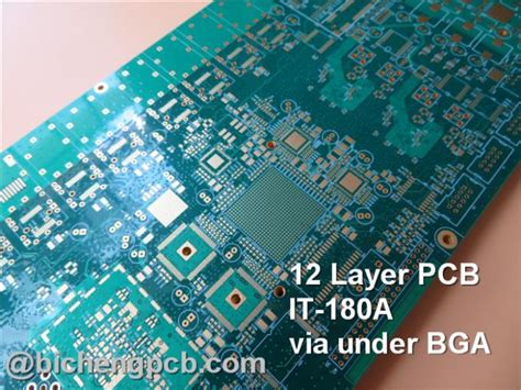
High Layer Count: HDI technology allows for the fabrication of boards with a higher number of layers, facilitating more complex designs and improved signal integrity.
-
Sequential Lamination: This process involves building up the PCB in multiple lamination steps, allowing for the creation of intricate structures and enhanced reliability.
Benefits of HDI PCBs
Space Savings and Miniaturization
One of the primary advantages of HDI PCBs is their ability to pack more functionality into a smaller space. The use of fine line widths, microvias, and high-density component placement enables designers to create compact, lightweight devices without sacrificing performance. This is particularly beneficial in applications where size and weight are critical factors, such as mobile devices, wearables, and aerospace systems.
Improved Electrical Performance
HDI PCBs offer several electrical performance benefits compared to traditional PCBs:
-
Reduced Signal Interference: The closer proximity of components and shorter signal paths in HDI designs help minimize crosstalk and electromagnetic interference (EMI), resulting in cleaner, more stable signals.
-
Enhanced Signal Integrity: The use of controlled impedance design techniques and the ability to place decoupling capacitors closer to ICs help maintain signal integrity, reducing noise and improving overall system performance.
-
Lower Power Consumption: Shorter signal paths and reduced parasitic capacitance and inductance in HDI PCBs lead to lower power consumption, which is essential for battery-powered devices and energy-efficient systems.
Increased Reliability
HDI PCBs are known for their superior reliability compared to traditional PCBs. The use of microvias and sequential lamination processes helps create more robust and durable interconnections between layers, reducing the risk of delamination and other manufacturing defects. Additionally, the smaller size and weight of HDI boards make them less susceptible to mechanical stress and vibration, further enhancing their reliability in demanding environments.

HDI PCB Design Considerations
Designing HDI PCBs requires careful consideration of several factors to ensure optimal performance, manufacturability, and cost-effectiveness.
Layer Stack-up and Via Types
Choosing the appropriate layer stack-up and via types is crucial in HDI PCB design. The number of layers, their arrangement, and the use of blind, buried, and microvias should be determined based on the specific requirements of the application, such as signal integrity, power distribution, and component placement.
Here is an example of a typical HDI PCB layer stack-up:
| Layer | Description |
|---|---|
| Top Layer | Signal layer with fine line widths and microvias |
| Ground Plane | Solid ground plane for EMI shielding and signal integrity |
| Signal Layer 1 | Signal layer with blind and buried vias |
| Signal Layer 2 | Signal layer with blind and buried vias |
| Power Plane | Solid power plane for stable power distribution |
| Signal Layer 3 | Signal layer with blind and buried vias |
| Signal Layer 4 | Signal layer with blind and buried vias |
| Bottom Layer | Signal layer with fine line widths and microvias |
Component Selection and Placement
When designing HDI PCBs, it is essential to select components that are compatible with the fine pitch and high-density requirements of the board. Surface mount devices (SMDs) with small package sizes, such as chip-scale packages (CSPs) and ball grid arrays (BGAs), are commonly used in HDI designs.
Component placement should be optimized to minimize signal path lengths, reduce crosstalk, and facilitate efficient routing. Designers should also consider the thermal management requirements of the components and incorporate appropriate heat dissipation techniques, such as thermal vias and heat sinks.
Signal Integrity and Power Integrity Analysis
To ensure optimal performance, HDI PCB designers must conduct thorough signal integrity (SI) and power integrity (PI) analyses. SI analysis involves simulating and evaluating the behavior of signals as they propagate through the board, taking into account factors such as impedance matching, crosstalk, and reflections. PI analysis focuses on the distribution of power throughout the board, ensuring that each component receives a stable and clean power supply.
These analyses help identify potential issues early in the design process, allowing for necessary adjustments to be made before fabrication, ultimately saving time and costs.
Design for Manufacturing (DFM)
Designing HDI PCBs with manufacturability in mind is crucial for ensuring a smooth and cost-effective production process. Designers should adhere to the manufacturing capabilities and guidelines provided by the chosen PCB fabricator, including minimum line widths, spacings, via sizes, and drill hole tolerances.
Other DFM considerations include:
- Avoiding acute angles in trace routing to prevent acid traps during etching
- Providing sufficient clearance between components and traces to facilitate assembly
- Incorporating fiducial markers for accurate component placement
- Using standard via sizes and pad geometries to reduce manufacturing complexity
By following DFM principles, designers can minimize the risk of manufacturing defects, improve yield rates, and reduce overall production costs.

HDI PCB Manufacturing Process
The manufacturing process for HDI PCBs involves several advanced techniques and technologies that enable the creation of high-density, multi-layer boards with fine features and intricate structures.
Laser Drilling
One of the key processes in HDI PCB manufacturing is laser drilling, which is used to create microvias. Unlike traditional mechanical drilling, laser drilling uses a focused, high-energy beam to vaporize the dielectric material, creating precise, small-diameter holes. This process allows for the creation of vias with diameters as small as 50 microns (2 mils), enabling higher interconnect density and more efficient use of board space.
Sequential Lamination
HDI PCBs are often manufactured using a sequential lamination process, which involves building up the board layer by layer. This process allows for the creation of complex structures, such as blind and buried vias, and enables the use of different materials for each layer, optimizing the board’s electrical and mechanical properties.
The sequential lamination process typically involves the following steps:
- Laminating a core layer with copper foil on both sides
- Drilling and plating through-holes
- Patterning and etching the outer layers
- Laminating additional layers with prepreg (pre-impregnated) material
- Laser drilling microvias
- Plating the microvias and patterning the new layers
- Repeating steps 4-6 until the desired number of layers is achieved
Advanced Materials
HDI PCBs often require the use of advanced materials to achieve the desired electrical and mechanical properties. Some common materials used in HDI manufacturing include:
-
Low-Dk and low-Df laminates: These materials have lower dielectric constant (Dk) and dissipation factor (Df) values, which help reduce signal loss and improve signal integrity at high frequencies.
-
High-Tg laminates: Materials with higher glass transition temperatures (Tg) offer better thermal stability and resistance to deformation during the assembly process, making them suitable for HDI boards with fine-pitch components.
-
Thin copper foils: Using thinner copper foils (e.g., 1/2 oz or 9 microns) allows for finer line widths and spaces, enabling higher circuit density and improved signal performance.
-
Low-CTE materials: Laminates with low coefficients of thermal expansion (CTE) help minimize stress and warpage during temperature changes, improving the reliability of HDI boards.
Quality Control and Testing
Ensuring the quality and reliability of HDI PCBs requires stringent quality control measures and comprehensive testing throughout the manufacturing process. Some common quality control and testing methods include:
-
Automated optical inspection (AOI): Used to detect surface defects, such as shorts, opens, and misaligned components.
-
X-ray inspection: Helps identify internal defects, such as voids in vias, delamination, and poor solder joints.
-
Electrical testing: Includes continuity testing, insulation resistance testing, and high-potential (hipot) testing to verify the electrical integrity of the board.
-
Microsectioning: Involves cross-sectioning the board and examining it under a microscope to assess the quality of plating, lamination, and other internal structures.
By implementing rigorous quality control and testing procedures, manufacturers can ensure that HDI PCBs meet the required specifications and performance standards, minimizing the risk of failures in the field.

Applications of HDI PCBs
HDI PCBs find applications in a wide range of industries and products, particularly those that demand high performance, miniaturization, and reliability. Some notable applications include:
Consumer Electronics
HDI technology is extensively used in consumer electronics, such as smartphones, tablets, laptops, and wearables. These devices require compact, lightweight designs with advanced features and functionality, making HDI PCBs an ideal choice. The high-density interconnects and fine-pitch components enable the integration of powerful processors, high-resolution displays, and multiple sensors in a small form factor.
Telecommunications
The telecommunications industry heavily relies on HDI PCBs for the development of advanced networking equipment, such as routers, switches, and base stations. These boards enable the design of high-speed, high-bandwidth systems that can handle the increasing demand for data transmission and processing. HDI technology also facilitates the implementation of advanced features, such as beamforming and massive MIMO (multiple-input, multiple-output), in 5G networks.
Aerospace and Defense
HDI PCBs are essential in aerospace and defense applications, where reliability, performance, and size are critical factors. These boards are used in avionics systems, satellite communications, radar systems, and military equipment. HDI technology enables the design of rugged, compact, and lightweight systems that can withstand harsh environments and extreme temperature ranges.
Medical Devices
The medical device industry is another significant adopter of HDI technology. HDI PCBs are used in a variety of medical applications, including implantable devices, diagnostic equipment, and patient monitoring systems. The high-density interconnects and fine-pitch components enable the design of miniaturized, high-performance devices that can improve patient comfort and outcomes.
Automotive Electronics
As vehicles become increasingly sophisticated, with advanced driver assistance systems (ADAS), infotainment systems, and electrification, HDI PCBs play a crucial role in automotive electronics. These boards enable the integration of multiple sensors, processors, and communication modules in a compact, reliable package, facilitating the development of safer, more efficient, and feature-rich vehicles.
FAQ
-
Q: What is the difference between HDI PCBs and traditional PCBs?
A: HDI PCBs have finer line widths, smaller via holes, and higher component density compared to traditional PCBs. This enables HDI boards to offer superior electrical performance, increased functionality, and smaller form factors. -
Q: What are the main benefits of using HDI PCBs?
A: The main benefits of HDI PCBs include space savings and miniaturization, improved electrical performance, and increased reliability. These advantages make HDI technology suitable for a wide range of applications that require high performance, compact designs, and robustness. -
Q: What are microvias, and why are they important in HDI PCBs?
A: Microvias are small, laser-drilled holes with diameters less than 150 microns (5.9 mils) that enable interconnections between layers in HDI PCBs. They are important because they allow for higher interconnect density and more efficient use of board space, facilitating the design of compact, high-performance devices. -
Q: What industries commonly use HDI PCBs?
A: HDI PCBs are commonly used in various industries, including consumer electronics, telecommunications, aerospace and defense, medical devices, and automotive electronics. These industries require advanced, miniaturized, and reliable electronic systems that can benefit from HDI technology. -
Q: What are some key considerations when designing HDI PCBs?
A: When designing HDI PCBs, key considerations include choosing the appropriate layer stack-up and via types, selecting compatible components and optimizing their placement, conducting thorough signal and power integrity analyses, and adhering to design for manufacturing (DFM) principles to ensure a cost-effective and reliable production process.
Conclusion
High-Density Interconnect (HDI) Printed Circuit Boards have revolutionized the electronics industry by enabling the design of compact, high-performance, and reliable devices. With their fine line widths, small via holes, and high component density, HDI PCBs offer numerous benefits, including space savings, improved electrical performance, and increased reliability.
The growing demand for miniaturization and advanced functionality in various industries, such as consumer electronics, telecommunications, aerospace, and medical devices, has fueled the adoption of HDI technology. To successfully design and manufacture HDI PCBs, engineers must consider factors such as layer stack-up, component selection and placement, signal and power integrity, and design for manufacturing principles.
As electronic devices continue to evolve and become more sophisticated, the importance of HDI PCBs will only continue to grow. By staying at the forefront of HDI technology and best practices, engineers and manufacturers can create innovative, high-quality products that meet the ever-increasing demands of the market.


Leave a Reply