What are Vias?
Vias are small holes drilled through a printed circuit board (PCB) that allow electrical connections between different layers of the board. They are an essential part of PCB design, enabling complex circuits to be routed efficiently in a compact space. However, vias also present some challenges in PCB manufacturing and assembly. This article will explore three key techniques related to vias: tenting, plugging, and via-in-pad.
Types of Vias
There are several different types of vias used in PCB design:
| Via Type | Description |
|---|---|
| Through hole via | Drilled completely through the PCB, connecting all layers |
| Blind via | Connects an outer layer to an inner layer, but does not go through the entire board |
| Buried via | Connects two or more inner layers, with no connection to the outer layers |
| Microvia | A small via, typically laser drilled, used for high-density interconnect (HDI) designs |
The choice of via type depends on the complexity and requirements of the PCB design.
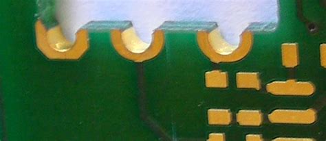
What is Via Tenting?
Via tenting is a process where the Via holes are covered or “tented” with solder mask on one or both sides of the PCB. This is done to prevent solder from flowing into the via during the assembly process, which could cause short circuits or other issues.
Advantages of Via Tenting
- Prevents solder from flowing into the via during reflow
- Provides a cleaner, more aesthetic appearance on the finished board
- Can help to strengthen the mechanical structure of the PCB
- May reduce the risk of contamination or corrosion in the via
Disadvantages of Via Tenting
- Can make it more difficult to inspect or repair connections at the via location
- May increase the capacitance of the via, which could impact high-frequency signal integrity
- Requires precise control of solder mask application to ensure proper coverage
Via Tenting Process
The via tenting process typically involves the following steps:
- Drilling: Via holes are drilled through the PCB substrate.
- Plating: The via holes are plated with a conductive material, usually copper.
- Solder Mask Application: A layer of solder mask is applied over the entire PCB surface, including the via locations.
- Solder Mask Exposure: The solder mask is exposed to UV light through a photomask, which hardens the mask in the desired areas.
- Solder Mask Development: The unexposed solder mask is removed, leaving the via holes covered or “tented.”
The specific parameters of the via tenting process, such as the solder mask material, thickness, and exposure time, may vary depending on the PCB manufacturer and the requirements of the design.

What are Plugged Vias?
Plugged vias, also known as filled vias, are vias that have been completely filled with a non-conductive material, such as epoxy resin. This is done to create a smooth, flat surface on the PCB, which can be important for certain manufacturing processes or applications.
Advantages of Plugged Vias
- Provides a completely smooth and flat surface on the PCB
- Eliminates the risk of solder flowing into the via during assembly
- Can improve the mechanical strength and durability of the PCB
- May enhance thermal conductivity, depending on the fill material used
Disadvantages of Plugged Vias
- Adds complexity and cost to the PCB manufacturing process
- May impact signal integrity, especially for high-frequency designs
- Can be difficult to rework or repair if issues arise
Via Plugging Process
The via plugging process typically involves the following steps:
- Drilling: Via holes are drilled through the PCB substrate.
- Plating: The via holes are plated with a conductive material, usually copper.
- Filling: The via holes are filled with a non-conductive material, such as epoxy resin.
- Curing: The fill material is cured, typically using heat or UV light.
- Planarization: The excess fill material is removed through sanding or other methods to create a smooth, flat surface.
The choice of fill material and the specific parameters of the via plugging process can impact the performance and reliability of the PCB.

What is Via-in-Pad?
Via-in-pad, also known as via-in-land, is a technique where a via is placed directly within a component pad on the PCB. This allows for more efficient use of board space and can simplify routing in dense designs.
Advantages of Via-in-Pad
- Enables higher density PCB layouts by saving space
- Can simplify routing and reduce the number of PCB Layers required
- Provides a direct connection between the component and the via
- May improve signal integrity by reducing the stub length
Disadvantages of Via-in-Pad
- Requires precise alignment and control during the assembly process
- Can be more susceptible to solder joint defects, such as voids or incomplete filling
- May impact the mechanical strength of the solder joint
- Can be more difficult to rework or repair if issues arise
Via-in-Pad Design Considerations
When designing a PCB with via-in-pad, several factors must be considered:
- Pad size: The pad must be large enough to accommodate both the component lead and the via.
- Via size: The via should be sized appropriately for the current and signal requirements of the connection.
- Solder mask: Solder mask can be used to tent the via, preventing solder from flowing into it during reflow.
- Fill material: If the via is filled, the choice of fill material can impact the performance and reliability of the connection.
Proper design and manufacturing controls are essential to ensure the success of via-in-pad techniques in PCB Assembly.

FAQ
Q1: What is the difference between tenting and plugging vias?
A1: Via tenting involves covering the via holes with solder mask, while via plugging involves completely filling the vias with a non-conductive material. Tenting provides a protective cover, while plugging creates a smooth, flat surface.
Q2: Can via tenting be used with via-in-pad designs?
A2: Yes, via tenting is often used in conjunction with via-in-pad to prevent solder from flowing into the via during the assembly process. This helps to ensure a reliable solder joint between the component and the pad.
Q3: What materials are commonly used for via plugging?
A3: Epoxy resin is a common material used for via plugging, due to its good mechanical and thermal properties. Other materials, such as conductive pastes or polymers, may also be used depending on the specific requirements of the application.
Q4: How does via-in-pad impact signal integrity?
A4: Via-in-pad can improve signal integrity by providing a direct connection between the component and the via, reducing the stub length. However, the presence of the via within the pad can also impact the impedance and capacitance of the connection, which may need to be accounted for in the design.
Q5: Are there any special considerations for testing PCBs with plugged vias?
A5: Plugged vias can present challenges for some testing methods, such as bed-of-nails testing or flying probe testing, as the test probes may not be able to make direct contact with the vias. Alternative testing methods, such as boundary scan or X-ray inspection, may be required for PCBs with plugged vias.
Conclusion
Tenting vias, plugging vias, and via-in-pad are all techniques used in PCB design and manufacturing to address specific challenges related to vias. Each method has its own advantages and disadvantages, and the choice of which to use depends on the specific requirements of the PCB design and application.
Via tenting provides a protective cover for vias, preventing solder from flowing into them during assembly. Via plugging completely fills the vias, creating a smooth, flat surface on the PCB. Via-in-pad allows for more efficient use of board space and can simplify routing in dense designs.
Designers and manufacturers must carefully consider the trade-offs and design considerations associated with each technique to ensure the best possible performance and reliability of the finished PCB. By understanding the benefits and limitations of via tenting, plugging, and via-in-pad, PCB professionals can make informed decisions and optimize their designs for success.


Leave a Reply