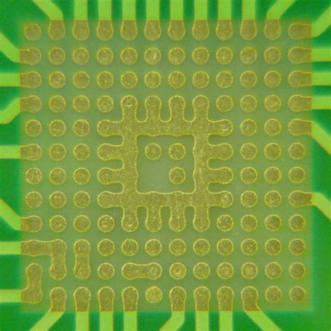
What are Vias?
Before diving into the topic of Plugged Vias, it’s essential to understand what vias are and their role in PCB design. Vias are small holes drilled through a PCB that allow for electrical connections between different layers of the board. They are typically plated with a conductive material, such as copper, to ensure a reliable electrical connection.
Vias come in different types, including:
- Through-hole vias: These vias go through all layers of the PCB.
- Blind vias: These vias connect an outer layer to an inner layer but do not go through the entire board.
- Buried vias: These vias connect inner layers without reaching the outer layers of the PCB.
What are Plugged Vias?
Plugged vias, also known as filled vias, are vias that have been filled with a non-conductive material, such as epoxy or resin. The primary purpose of plugging vias is to prevent the flow of liquid or gaseous substances through the via holes, which can cause contamination or damage to the PCB.
Reasons for Plugging Vias
There are several reasons why PCB designers and manufacturers choose to plug vias:
-
Preventing Contamination: In certain applications, such as medical devices or automotive electronics, it’s crucial to prevent contamination from entering the PCB through the via holes. Plugging the vias helps maintain a sealed environment and protects the board from external contaminants.
-
Improving Structural Integrity: Plugging vias can enhance the structural integrity of the PCB, especially in applications where the board is subjected to mechanical stress or vibration. The filled vias provide additional support and reduce the risk of via fatigue or cracking.
-
Enhancing Thermal Management: In high-power applications, plugged vias can help dissipate heat more efficiently. The non-conductive material used to fill the vias can have a higher thermal conductivity than air, allowing for better heat transfer from the PCB to the surrounding environment.
-
Facilitating Conformal Coating: When applying a conformal coating to a PCB, plugged vias can prevent the coating material from seeping into the via holes and potentially causing short circuits or other issues.
Drawbacks of Plugging Vias
While plugging vias offers several benefits, there are also some drawbacks to consider:
-
Increased Manufacturing Cost: Plugging vias adds an extra step to the PCB manufacturing process, which can increase production time and cost. The materials used for plugging, such as epoxy or resin, also contribute to the overall cost of the PCB.
-
Potential for Voids: If the via plugging process is not carefully controlled, it can result in the formation of voids or air pockets within the filled vias. These voids can compromise the structural integrity and thermal management properties of the plugged vias.
-
Reduced Electrical Performance: In some cases, plugging vias can negatively impact the electrical performance of the PCB. The non-conductive material used for plugging can have a higher dielectric constant than air, which can affect signal integrity and increase capacitance.

Via Plugging Techniques
There are several techniques used for plugging vias, each with its own advantages and limitations:
Epoxy Filling
Epoxy filling involves using a liquid epoxy resin to fill the via holes. The epoxy is typically applied using a dispensing machine or a screen printing process. Once applied, the epoxy is cured using heat, UV light, or a combination of both.
Advantages:
– Provides a strong, durable fill
– Can be used for high-aspect-ratio vias
– Offers good thermal conductivity
Limitations:
– Requires specialized equipment for application
– Can be time-consuming and expensive
– Potential for voids if not properly controlled
Conductive Ink Filling
Conductive ink filling uses a conductive paste or ink to fill the via holes. The conductive material is typically a mixture of metal particles, such as silver or copper, suspended in a polymer binder. The ink is applied using a screen printing process and then cured using heat.
Advantages:
– Provides electrical conductivity
– Can be used for high-aspect-ratio vias
– Relatively low cost compared to other methods
Limitations:
– Lower thermal conductivity than epoxy filling
– Potential for voids or inconsistent filling
– May require multiple passes to achieve complete filling
Copper Plating
Copper plating involves electroplating additional copper onto the walls of the via holes until they are completely filled. This method is often used in conjunction with other filling techniques to ensure a complete and void-free fill.
Advantages:
– Provides excellent electrical conductivity
– Offers good thermal conductivity
– Ensures a complete and void-free fill
Limitations:
– Requires specialized plating equipment
– Can be time-consuming and expensive
– Limited to lower aspect ratio vias

Is Plugging Your Vias Necessary?
The decision to plug vias depends on several factors, including the specific application, the PCB’s operating environment, and the desired performance characteristics. In some cases, plugging vias is essential to ensure proper functionality and reliability, while in others, it may be an unnecessary expense.
Consider the following factors when deciding whether to plug your vias:
-
Application Requirements: If your PCB will be used in an environment where contamination or exposure to liquids or gases is a concern, plugging vias is highly recommended. Examples include medical devices, automotive electronics, and aerospace applications.
-
Structural Integrity: If your PCB will be subjected to mechanical stress or vibration, plugging vias can help improve its structural integrity and reduce the risk of via fatigue or cracking.
-
Thermal Management: In high-power applications where efficient heat dissipation is crucial, plugged vias can provide better thermal management than open vias.
-
Conformal Coating: If you plan to apply a conformal coating to your PCB, plugging vias can prevent the coating material from seeping into the via holes and causing issues.
-
Cost Considerations: Plugging vias adds cost to the PCB manufacturing process. If your application does not require plugged vias for proper functionality or reliability, you may choose to leave them unplugged to reduce costs.

Frequently Asked Questions (FAQ)
-
Q: Can all vias be plugged?
A: In general, most vias can be plugged. However, the feasibility of plugging depends on factors such as the via’s size, aspect ratio, and the plugging method used. High-aspect-ratio vias (depth-to-diameter ratio greater than 10:1) can be more challenging to plug completely. -
Q: What materials are commonly used for plugging vias?
A: The most common materials used for plugging vias are epoxy resins and conductive inks. Epoxy resins provide a strong, durable fill with good thermal conductivity, while conductive inks offer electrical conductivity and are relatively low cost. -
Q: How does via plugging affect signal integrity?
A: Via plugging can have both positive and negative effects on signal integrity. On one hand, plugged vias can reduce the risk of signal reflections and crosstalk by providing a more controlled impedance environment. On the other hand, the non-conductive material used for plugging can have a higher dielectric constant than air, which can increase capacitance and affect signal integrity. -
Q: Can plugged vias be used for thermal management?
A: Yes, plugged vias can be used for thermal management in high-power applications. The non-conductive material used for plugging, such as epoxy, can have a higher thermal conductivity than air, allowing for better heat transfer from the PCB to the surrounding environment. -
Q: Are there any industry standards for via plugging?
A: While there are no specific industry standards for via plugging, various organizations, such as the IPC (Association Connecting Electronics Industries), provide guidelines and best practices for PCB manufacturing, including via plugging. The IPC-4761 standard, for example, covers the design, fabrication, and testing of protection and packaging of printed boards, including via protection methods.
Conclusion
Plugged vias are a valuable tool in PCB design and manufacturing, offering benefits such as contamination prevention, improved structural integrity, enhanced thermal management, and facilitation of conformal coating. However, the decision to plug vias depends on the specific application, operating environment, and desired performance characteristics of the PCB.
When considering via plugging, it’s essential to weigh the benefits against the potential drawbacks, such as increased manufacturing costs, the potential for voids, and reduced electrical performance in some cases. By understanding the various via plugging techniques and their advantages and limitations, PCB designers and manufacturers can make informed decisions about when and how to use plugged vias in their projects.
Ultimately, the necessity of plugging vias depends on the unique requirements of each PCB application. By carefully evaluating these requirements and working closely with experienced PCB manufacturers, designers can ensure that their boards are optimized for reliability, performance, and cost-effectiveness.


Leave a Reply