Introduction
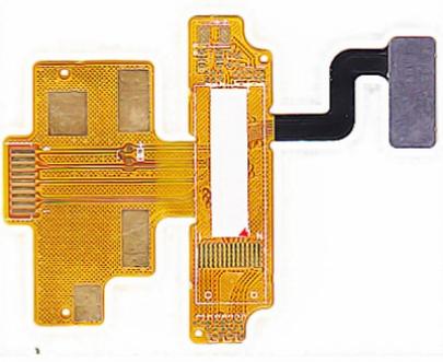
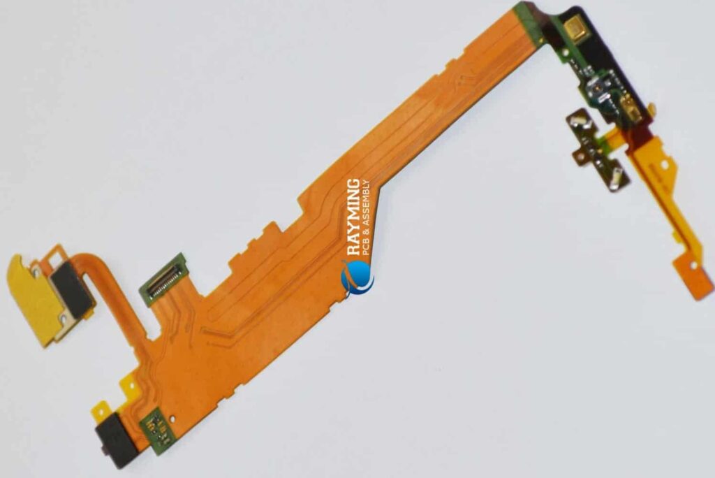
Flex PCBs, short for flexible printed circuit boards, are made from flexible dielectric materials like polyimide that allow the board to bend and flex. They are useful for applications where the circuit needs to move or adapt to different shapes. However, for some applications, the flex PCB may need additional stiffness and rigidity in certain areas while retaining flexibility in others. This is where stiffener flex PCBs come into play.
Stiffener flex PCBs contain regions of stiffeners, usually made from rigid FR4 material, bonded to the flex PCB. The stiffeners provide mechanical support and prevent unwanted bending in designated areas, while allowing flexibility in other areas. Proper design and integration of stiffeners are crucial to create a flex PCB that meets the specific mechanical and electrical requirements.
This article provides a detailed guide on stiffener flex PCB design and manufacturing considerations.
Benefits of Using Stiffeners on Flex PCBs
There are several key benefits of selectively reinforcing flex PCBs with stiffeners:
- Prevent Excessive Bending: Stiffeners can prevent mechanical failures like cracking by limiting bending in vulnerable areas. This ensures the reliability and lifespan of the product.
- Improve Component Stability: Components like connectors or switches mounted on stiffener areas will be more stable and resistant to vibration or shock.
- Facilitate Handling: Stiffened sections make the flex PCB easier to hold and install without causing damage.
- Reduce Warping: Stiffeners prevent warping of the flex PCB material due to temperature changes during soldering or operation.
- Simplify Assembly: A stiffened section allows easier assembly of multiple layer flex stacks aligned using precision locators.
- Improve Heat Dissipation: The stiffener acts as a heat spreader from high power components, improving thermal management.
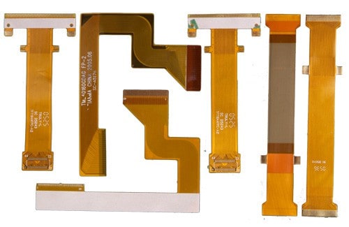
Stiffener Materials and Construction
Stiffeners are typically made from rigid FR4 material, but there are some other options as well:
- FR4: Glass-reinforced epoxy laminate. Most common due to good strength, temperature resistance, cost.
- Polyimide: Can match coefficient of expansion of flex PCB better. Less rigid than FR4.
- Aluminum: Excellent stiffness. Allows heat sinking. Higher cost.
- Stainless Steel: Very rigid with good temperature resistance. Heavier than other options.
The stiffener can be attached to the flex PCB in several ways:
- Bonded: Acrylic or epoxy adhesive. Simple but less rugged.
- Soldered: Reflowed solder interconnect. Requires plating on stiffener.
- Mechanically Fastened: Screws, rivets or clips. Bulky but allows disassembly.
- Molded: Plastic molded over or around the stiffener. Light and robust but complex process.
Stiffener Layout Design Guidelines
Careful design of the stiffener layout is key to achieving the desired mechanical performance while avoiding potential issues. Here are some important guidelines:
- Place stiffeners to prevent bending along the flexible circuit folds and around fragile components. Avoid overlapped stiffeners.
- Use the minimum size and thickness stiffener possible to maintain flexibility. Balance strength and rigidity requirements.
- Extend stiffeners beyond soldered components spans to distribute stresses. Allow sufficient border around mounts.
- Avoid placing stiffeners over flexing zones or folding joints which can crack rigid-flex interfaces.
- Include cutouts and holes in stiffener to facilitate bending where required. Slotted stiffeners are useful.
- Minimize number of different stiffener profiles to simplify assembly. Standardize placement and alignment where possible.
- Account for stiffener thickness when routing traces. Ensure adequate flex dielectric clearance.
Effects of Stiffeners on Flex PCB Assembly
Stiffeners impact certain aspects of the flex PCB assembly process:
- Stiffeners may be populated separately before final assembly. Use locator holes for alignment.
- Soldering requires pre-heating stiffener areas first then reflowing adjacent flex zones to prevent cracking.
- Adhesives under stiffeners may require longer cure time during assembly. Heat can also degrade bonds.
- Additional clamping, support or fixturing may be needed to hold stiffeners during assembly steps.
- Automated optical inspection requires separate programs tuned for rigid and flex regions.
- Bulky stiffeners may obstruct transport and feeding through pick and place machines.
Understanding these effects is important to optimize assembly yield rate and throughput.
Thermal Considerations for Stiffener Flex PCBs
Since stiffeners conduct and spread heat, their design affects the thermal performance:
- Minimize stiffener area covering ground/power planes to limit thermal coupling and reduce heat spreading.
- Incorporate thermal reliefs and isolations gaps to control heat flow if needed. Avoid large contiguous stiffeners.
- Place individual stiffeners at components with high thermal pad connections to sink heat.
- Use thermal vias under stiffeners to provide heat conduction paths to inner ground planes if required.
- Increased thermal stresses can develop between stiffener-flex interfaces. Manage with materials with matched CTE.
Careful thermal design is necessary to prevent detrimental impacts on circuit performance or reliability.
Electrical Design Rules for Stiffener Integration
Integrating stiffeners requires special considerations for routing and layer stackup:
Layer Stackup
- Reference planes under stiffeners should extend under adjacent flex areas for stability. Use bridges to connect planes across cuts.
- Include at least one ground plane layer if stiffener does not have its own reference planes.
- Ensure microstrip trace impedances are maintained across stiffener-flex transitions.
Trace Routing
- Do not route traces over stiffener-flex boundary. Stress can fracture traces. Provide clearance of ~1-2 mm.
- For traces crossing stiffener slots, use teardrops to distribute stress gradually.
- Impedance match traces when transitioning from thick stiffener to thinner flex layers.
- Adjust length of traces crossing slots to account for elongation during flexing.
Following appropriate guidelines will help avoid problems during circuit fabrication.
Stiffener and Flex PCB Design Checklist
Here is a summary checklist of key design considerations when working with stiffener flex PCBs:
- Define locations requiring stiffeners for mechanical support or stability.
- Select optimal stiffener materials based on strength, rigidity, and fabrication requirements.
- Design stiffener layout with appropriate positioning, thickness, cutouts and edge margins.
- Adjust PCB layer stackup with proper plane design and dielectric materials.
- Ensure electrical rules are followed for traces crossing stiffeners and slots.
- Account for impacts on assembly process such as clamping, heating, and inspection.
- Analyze thermal heat flow and incorporate features to manage temperature effects.
- Work closely with your PCB manufacturer during design reviews to finalize details.
Thorough planning and collaboration will result in a robust stiffener flex PCB optimized for the application.
Quality Control and Testing
Rigorous quality control and testing helps ensure stiffener flex PCBs meet specifications:
- Materials and laminate quality control assures consistent material properties.
- CTE and modulus testing verifies suitability for thermal stresses.
- Adhesion pulls tests check integrity of stiffener bonds and material interfaces.
- Microsectioning and microscopy detects any layer separation issues or cracks.
- HAST, temperature cycling, and bend cycle testing assess reliability under stresses.
- Automated optical inspection of trace separations, drill quality, and solder joints.
- Net dimension and stiffener profile measurements validate mechanical precision.
- Electrical impedance and signal integrity measurements guarantee circuit performance.
A well-defined quality and qualification plan applied through the fabrication workflow minimizes potential defects in the finished product.
Frequently Asked Questions
What are some typical applications of stiffener flex PCBs?
Some common applications include wearable devices, display assemblies, camera modules, lidar sensors, robotic arms, and medical electronics where controlled flexing and rigidity are required.
How are components assembled onto stiffener sections of the PCB?
Surface mount components can be directly soldered onto the stiffener areas using standard SMT assembly processes. For through hole components, cutouts in the stiffener may be required for leads.
Can existing standard flex PCB designs be modified to include stiffeners?
Yes, introducing stiffeners to current flex PCB designs is possible but may require adjustments to layer stackup, thermal management, and sometimes layout to integrate the stiffeners appropriately.
What types of computer simulation can help in modeling stiffener flex PCBs?
FEA software is useful for modeling mechanical stress distribution. Thermal modeling tools also provide simulation capabilities to optimize heat flow for reliability. Impedance analysis can verify electrical performance.
How are very small or complex shaped stiffeners integrated onto the flex PCB?
For small or intricate stiffener patterns, techniques like laser cutting, die-cutting or chemical etching allow precise stiffener formation and integration during lamination.
Conclusion
Stiffener flex PCBs provide the ideal combination of mechanical stability and rigidity in designated regions while retaining flexibility where needed. Correct incorporation of stiffeners requires careful consideration of layout, electrical performance, assembly factors, and thermal effects. With robust design and process controls, stiffener flex PCBs can enable miniaturized and reliable products in demanding applications. Continued advancements in materials, modeling tools, and manufacturing techniques will drive further innovation in this important technology.


Leave a Reply