What is Solder Mask Material?
Solder mask, also known as solder resist or solder stop, is a thin layer of polymer applied to the copper traces of a printed circuit board (PCB) to protect them from oxidation, prevent solder bridges, and provide electrical insulation. This material is essential in the manufacturing process of PCBs, as it ensures the reliability and longevity of the final product.
Types of Solder Mask Materials
There are two main types of solder mask materials:
-
Liquid Photoimageable Solder Mask (LPSM): This type of solder mask is applied as a liquid and then exposed to UV light through a photomask to cure and harden the material. LPSM offers excellent resolution and is suitable for high-density PCBs.
-
Dry Film Solder Mask (DFSM): DFSM is a solid film that is laminated onto the PCB surface using heat and pressure. After lamination, the film is exposed to UV light through a photomask and developed to remove the unexposed areas. DFSM is more cost-effective and easier to apply than LPSM.
| Property | Liquid Photoimageable Solder Mask (LPSM) | Dry Film Solder Mask (DFSM) |
|---|---|---|
| Application Method | Liquid, screen printed or sprayed | Solid film, laminated |
| Resolution | High | Medium to High |
| Cost | Higher | Lower |
| Ease of Use | More complex | Simpler |
| Suitable for | High-density PCBs | Medium to high-density PCBs |
Properties of Solder Mask Material
A good solder mask material should possess the following properties:
-
Electrical Insulation: Solder mask should provide excellent electrical insulation to prevent short circuits and ensure the proper functioning of the PCB.
-
Chemical Resistance: The material should be resistant to various chemicals, such as acids, alkalis, and solvents, to protect the copper traces from corrosion during the manufacturing process and in the final application.
-
Thermal Stability: Solder mask should withstand high temperatures during the soldering process without degrading or losing its properties.
-
Mechanical Strength: The material should have good mechanical strength to protect the copper traces from physical damage during handling and assembly.
-
Adhesion: Solder mask should adhere well to the PCB surface to prevent delamination and ensure long-term reliability.
Common Solder Mask Material Compositions
Solder mask materials are typically composed of the following components:
-
Resin: The main component of solder mask, providing the bulk of the material’s properties. Common resins include epoxy, acrylic, and polyurethane.
-
Fillers: Inorganic particles, such as silica or alumina, added to improve the mechanical and thermal properties of the solder mask.
-
Pigments: Color additives used to give the solder mask its distinctive color, typically green, red, blue, or black.
-
Photoinitiators: Compounds that initiate the polymerization reaction when exposed to UV light, causing the solder mask to cure and harden.
-
Solvents: Used to adjust the viscosity of the solder mask for optimal application.

Solder Mask Application Process
The solder mask application process varies depending on the type of material used, but the general steps are as follows:
-
Surface Preparation: The PCB surface is cleaned and treated to ensure good adhesion of the solder mask.
-
Solder Mask Application: The solder mask material is applied to the PCB surface using screen printing, spraying, or lamination, depending on the type of material.
-
Exposure: The applied solder mask is exposed to UV light through a photomask, causing the exposed areas to cure and harden.
-
Development: The unexposed areas of the solder mask are removed using a developer solution, revealing the copper traces that need to be soldered.
-
Curing: The PCB is heated to fully cure the solder mask and ensure its final properties.

Solder Mask Color Options
Solder mask is available in various colors, with green being the most common. Other popular colors include:
- Red
- Blue
- Black
- White
- Yellow
The choice of color is often a matter of preference or based on the specific application requirements. For example, white solder mask is sometimes used for LED lighting applications to enhance light reflection.

Solder Mask Finish Options
In addition to the standard glossy finish, solder mask can be produced with various surface finishes to suit specific requirements:
-
Matte Finish: A non-reflective surface that reduces glare and improves the readability of text and markings on the PCB.
-
Semi-Matte Finish: A compromise between glossy and matte finishes, offering some glare reduction while maintaining a slightly reflective appearance.
-
Textured Finish: A rough surface that provides better grip for handling and can help prevent slippage during assembly.
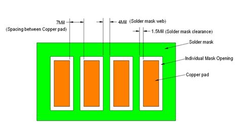
Solder Mask Design Considerations
When designing a PCB with solder mask, consider the following factors:
-
Clearance: Ensure adequate clearance between the solder mask and the copper traces to prevent solder bridging and allow for proper soldering.
-
Solder Mask Expansion: Account for the expansion of the solder mask during the curing process, which can slightly reduce the size of exposed copper areas.
-
Solder Mask Thickness: Choose an appropriate solder mask thickness based on the PCB’s application and the required level of protection.
-
Solder Mask Color: Select a solder mask color that provides good contrast with the copper traces and any text or markings on the PCB for easy identification and readability.
FAQ
-
Q: What is the purpose of solder mask on a PCB?
A: Solder mask serves three main purposes: protecting the copper traces from oxidation, preventing solder bridges between closely spaced traces, and providing electrical insulation. -
Q: Can solder mask be applied selectively to specific areas of a PCB?
A: Yes, solder mask can be selectively applied to certain areas of a PCB using the same photoimaging process used to pattern the copper traces. This allows for exposed copper areas where required, such as contact pads or test points. -
Q: Is solder mask required on all PCBs?
A: While solder mask is highly recommended for most PCBs, it is not always required. Some simple, low-density PCBs or those used in non-critical applications may forgo solder mask to reduce costs. -
Q: What is the typical thickness of solder mask on a PCB?
A: The typical thickness of solder mask ranges from 0.0005 to 0.002 inches (12.7 to 50.8 microns), depending on the specific material and application requirements. -
Q: Can solder mask be removed if needed?
A: Yes, solder mask can be removed using abrasive methods, such as sanding or scraping, or by using chemical solder mask strippers. However, removing solder mask should be done carefully to avoid damaging the underlying copper traces.
Conclusion
Solder mask is a critical material in the manufacturing of printed circuit boards, providing essential protection and insulation for the copper traces. By understanding the types, properties, and application processes of solder mask materials, PCB designers and manufacturers can ensure the production of high-quality, reliable PCBs that meet the specific requirements of their intended applications.


Leave a Reply