Introduction to SMT Stencils
Surface-mount technology (SMT) stencils are essential tools in the printed circuit board (PCB) assembly process. They are used to apply solder paste onto the PCB pads, ensuring precise and consistent solder paste deposition. SMT stencils come in various types, including framed, frameless, and step-up stencils, each with its own advantages and applications.
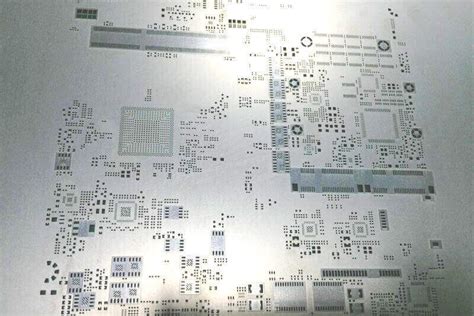
What are SMT Stencils?
SMT stencils are thin metal sheets with apertures that correspond to the PCB pads. They are placed on top of the PCB, and solder paste is applied using a squeegee. The solder paste is forced through the apertures, depositing it onto the PCB pads. The stencil is then removed, leaving the solder paste in the desired locations.
Importance of SMT Stencils in PCB Assembly
SMT stencils play a crucial role in the PCB assembly process for several reasons:
-
Precise solder paste deposition: SMT stencils ensure that the correct amount of solder paste is applied to each pad, preventing insufficient or excessive solder paste, which can lead to defects.
-
Consistent solder paste volume: By using a stencil, the solder paste volume is consistent across all pads, resulting in a more reliable and uniform soldering process.
-
Increased efficiency: SMT stencils enable the rapid application of solder paste to multiple PCBs, significantly reducing the time required for manual solder paste application.
-
Compatibility with various components: SMT stencils can be designed to accommodate a wide range of component sizes and types, from small chip components to large BGAs.
Types of SMT Stencils
There are three main types of SMT stencils: framed, frameless, and step-up stencils. Each type has its own characteristics, advantages, and applications.
Framed SMT Stencils
Framed SMT stencils are the most common type of stencil used in PCB assembly. They consist of a thin metal sheet (usually stainless steel) that is stretched and secured within a metal frame. The frame provides stability and rigidity to the stencil, making it easier to handle and position on the PCB.
Advantages of Framed SMT Stencils
-
Durability: The metal frame protects the stencil from damage during handling and storage, increasing its lifespan.
-
Ease of use: The frame makes it easier to align and position the stencil on the PCB, reducing the risk of misalignment and ensuring consistent solder paste deposition.
-
Compatibility with various printing systems: Framed stencils can be used with a wide range of Solder paste printing systems, including manual and automated systems.
Applications of Framed SMT Stencils
Framed SMT stencils are suitable for a wide range of PCB assembly applications, from prototype to high-volume production. They are particularly useful for PCBs with larger components and those requiring a higher degree of precision and consistency in solder paste deposition.
Frameless SMT Stencils
Frameless SMT stencils, also known as foilless stencils, consist of a thin metal sheet without a supporting frame. They are typically used in specialized applications where the frame may interfere with the solder paste printing process.
Advantages of Frameless SMT Stencils
-
Reduced stencil thickness: Without the added thickness of a frame, frameless stencils can be made thinner, allowing for finer pitch components and more precise solder paste deposition.
-
Improved flexibility: Frameless stencils are more flexible than framed stencils, making them suitable for applications where the stencil needs to conform to slight irregularities in the PCB surface.
-
Cost-effective: Frameless stencils are generally less expensive than framed stencils, as they require less material and manufacturing time.
Applications of Frameless SMT Stencils
Frameless SMT stencils are commonly used in applications involving fine-pitch components, such as chip-scale packages (CSPs) and ball grid arrays (BGAs). They are also useful for PCBs with limited space, where the frame of a conventional stencil may interfere with components or other features.
Step-Up SMT Stencils
Step-up SMT stencils, also known as multi-level or 3D stencils, feature apertures with different heights or steps. This allows for the deposition of varying amounts of solder paste on different areas of the PCB, accommodating components with different height requirements.
Advantages of Step-Up SMT Stencils
-
Improved solder paste volume control: Step-up stencils enable the precise control of solder paste volume for different component types, ensuring optimal solder joint formation.
-
Reduced solder bridging: By depositing the appropriate amount of solder paste for each component, step-up stencils minimize the risk of solder bridging between closely spaced pads.
-
Enhanced component reliability: With the correct solder paste volume for each component, step-up stencils contribute to improved component reliability and reduced defects.
Applications of Step-Up SMT Stencils
Step-up SMT stencils are particularly useful for PCBs with a mix of component types and sizes, such as those containing both small chip components and larger BGAs or connectors. They are also beneficial for applications requiring a high degree of solder joint reliability, such as automotive, aerospace, and medical electronics.

Stencil Material and Thickness
The choice of stencil material and thickness is crucial for achieving optimal solder paste deposition and ensuring the longevity of the stencil.
Stencil Material
The most common material used for SMT stencils is stainless steel, specifically grade 304 or 316. Stainless steel offers several advantages:
-
Durability: Stainless steel is resistant to wear and tear, ensuring a long stencil lifespan.
-
Corrosion resistance: Stainless steel is resistant to corrosion, preventing the formation of rust or other contaminants that could affect solder paste deposition.
-
Ease of cleaning: Stainless steel stencils are easy to clean, allowing for the efficient removal of solder paste residue between printing cycles.
Other materials, such as nickel and polyimide, may be used in specific applications, but stainless steel remains the most widely used material for SMT stencils.
Stencil Thickness
The thickness of an SMT stencil is a critical factor in determining the amount of solder paste deposited on the PCB pads. The appropriate stencil thickness depends on several factors, including the size and pitch of the components, the desired solder paste volume, and the PCB design.
Common stencil thicknesses range from 0.100 mm to 0.250 mm (4 to 10 mils). Thinner stencils are used for fine-pitch components and smaller solder paste volumes, while thicker stencils are used for larger components and greater solder paste volumes.
| Component Pitch | Recommended Stencil Thickness |
|---|---|
| < 0.5 mm | 0.100 – 0.125 mm (4 – 5 mils) |
| 0.5 – 0.8 mm | 0.125 – 0.150 mm (5 – 6 mils) |
| 0.8 – 1.27 mm | 0.150 – 0.200 mm (6 – 8 mils) |
| > 1.27 mm | 0.200 – 0.250 mm (8 – 10 mils) |
It is essential to consider the specific requirements of the PCB design and consult with the stencil manufacturer to determine the optimal stencil thickness for a given application.

Stencil Aperture Design
The design of the stencil apertures is crucial for achieving the desired solder paste deposition and ensuring the formation of reliable solder joints. Several factors must be considered when designing stencil apertures.
Aperture Size and Shape
The size and shape of the stencil apertures should be designed to match the size and shape of the PCB pads. The aperture dimensions are typically slightly larger than the pad dimensions to allow for proper solder paste release and to account for any misalignment during the printing process.
Common aperture shapes include:
-
Rectangle: Used for most surface-mount components, such as chip resistors, capacitors, and SOICs.
-
Square: Used for square-shaped pads, such as those found on QFNs and some connectors.
-
Circle: Used for round pads, such as those found on BGAs and some connectors.
-
Oblong: Used for elongated pads, such as those found on some connectors and power components.
The choice of aperture shape should be based on the shape of the PCB pads and the specific requirements of the components being used.
Aperture Wall Angle
The aperture wall angle, also known as the aperture sidewall angle, refers to the angle between the aperture wall and the stencil surface. The aperture wall angle affects the release of the solder paste from the stencil and the resulting solder paste deposit on the PCB pad.
Common aperture wall angles range from 0° to 30°. A smaller wall angle (closer to 0°) results in a more vertical aperture wall, which can improve solder paste release and deposit consistency. However, a smaller wall angle also increases the risk of stencil damage and reduces the stencil lifespan.
A larger wall angle (closer to 30°) results in a more tapered aperture wall, which can improve stencil durability and lifespan. However, a larger wall angle may result in less consistent solder paste deposits and may require more frequent stencil cleaning.
The choice of aperture wall angle should be based on the specific requirements of the PCB design, the solder paste being used, and the desired balance between solder paste deposit consistency and stencil durability.
Aperture Aspect Ratio
The aperture aspect ratio is the ratio of the aperture width to the stencil thickness. A higher aspect ratio (larger width relative to thickness) results in a larger solder paste deposit, while a lower aspect ratio (smaller width relative to thickness) results in a smaller solder paste deposit.
The optimal aperture aspect ratio depends on the specific requirements of the PCB design and the components being used. In general, an aspect ratio between 1.5 and 2.0 is considered suitable for most applications. However, for fine-pitch components or those requiring a smaller solder paste deposit, a lower aspect ratio may be necessary.
It is important to consider the aperture aspect ratio in conjunction with the stencil thickness and the desired solder paste volume to ensure optimal solder paste deposition and reliable solder joint formation.

Stencil Printing Process
The stencil printing process is a critical step in the PCB assembly process, as it directly affects the quality and reliability of the solder joints. Several factors must be considered to ensure a successful stencil printing process.
Solder Paste Selection
The selection of the appropriate solder paste is essential for achieving reliable solder joints. Solder paste consists of a mixture of metal alloy powder (typically tin, lead, and silver) and flux. The solder paste should be compatible with the PCB Surface Finish, the component metallization, and the stencil printing process.
Key considerations when selecting solder paste include:
-
Alloy composition: The alloy composition determines the melting temperature, wetting properties, and mechanical strength of the solder joints. Common alloy compositions include SAC305 (96.5% tin, 3% silver, 0.5% copper) and Sn63/Pb37 (63% tin, 37% lead).
-
Particle size: The particle size of the metal alloy powder affects the printing process and the resulting solder joint quality. Smaller particle sizes enable finer pitch printing and more consistent solder paste deposition.
-
Flux type: The flux type (e.g., rosin, no-clean, water-soluble) determines the cleaning requirements and the solder paste’s compatibility with the PCB and components.
-
Viscosity: The solder paste viscosity affects its flow properties and the resulting solder paste deposit. A higher viscosity paste is generally better suited for larger components and thicker stencils, while a lower viscosity paste is better for finer pitch components and thinner stencils.
Consult with the solder paste manufacturer and consider the specific requirements of the PCB design to select the most appropriate solder paste for a given application.
Stencil Alignment
Accurate stencil alignment is crucial for ensuring precise solder paste deposition on the PCB pads. Misalignment can result in insufficient or excessive solder paste deposition, leading to defects such as solder bridges, opens, or poor solder joint formation.
Stencil alignment can be achieved through various methods, including:
-
Manual alignment: For low-volume production or prototyping, manual alignment using alignment pins or fiducials can be sufficient.
-
Automatic alignment: For high-volume production, automatic alignment systems using vision systems and motorized stages can ensure consistent and accurate alignment.
-
Stencil frames with alignment features: Some stencil frames incorporate alignment features, such as pins or holes, that mate with corresponding features on the PCB or the solder paste printer, ensuring accurate alignment.
Regardless of the alignment method used, it is essential to regularly check and adjust the stencil alignment to maintain consistent solder paste deposition throughout the production run.
Squeegee Selection and Pressure
The squeegee is responsible for pushing the solder paste through the stencil apertures and onto the PCB pads. The selection of the appropriate squeegee and the application of the correct pressure are essential for achieving consistent solder paste deposition.
Squeegee blades are typically made from polyurethane or metal (e.g., stainless steel). Polyurethane squeegees are more flexible and conform better to the stencil surface, while metal squeegees are more durable and provide a sharper printing edge.
The hardness of the squeegee blade is also an important consideration. A harder squeegee blade provides a cleaner printing edge and is better suited for finer pitch applications, while a softer squeegee blade conforms better to the stencil surface and is better for larger components and thicker solder paste deposits.
Squeegee pressure affects the amount of solder paste deposited on the PCB pads. Too little pressure may result in insufficient solder paste deposition, while too much pressure may cause solder paste bleeding or stencil damage. The optimal squeegee pressure depends on factors such as the solder paste viscosity, stencil thickness, and aperture size.
Experimentation and fine-tuning of the squeegee selection and pressure may be necessary to achieve the desired solder paste deposition for a given PCB design and production setup.
Print Speed and Separation Speed
The print speed and separation speed are two critical parameters in the stencil printing process that affect the quality and consistency of the solder paste deposition.
Print speed refers to the speed at which the squeegee moves across the stencil surface. A slower print speed allows for more time for the solder paste to fill the stencil apertures, resulting in a more consistent solder paste deposit. However, a slower print speed also reduces the production throughput. Conversely, a faster print speed increases the production throughput but may result in less consistent solder paste deposition.
Separation speed refers to the speed at which the stencil is lifted away from the PCB after printing. A slower separation speed allows for a more controlled release of the solder paste from the stencil apertures, reducing the risk of solder paste slumping or bridging. However, a slower separation speed also increases the overall cycle time. A faster separation speed reduces the cycle time but may result in less controlled solder paste release and increased defects.
The optimal print speed and separation speed depend on various factors, including the solder paste properties, stencil design, and PCB layout. Experimentation and optimization may be necessary to find the best balance between solder paste deposition quality and production throughput for a given application.
Stencil Maintenance and Cleaning
Proper maintenance and cleaning of SMT stencils are essential for ensuring consistent solder paste deposition and extending the stencil lifespan. Solder paste residue, debris, and damage to the stencil apertures can all lead to defects in the printed solder paste.
Stencil Cleaning Methods
There are several methods for cleaning SMT stencils, each with its own advantages and considerations:
-
Manual cleaning: Manual cleaning involves wiping the stencil with a lint-free cloth or paper towel soaked in a cleaning solution. This method is suitable for small-scale production or quick cleaning between prints but may not be as effective for removing stubborn solder paste residue.
-
Ultrasonic cleaning: Ultrasonic cleaning uses high-frequency sound waves to agitate a cleaning solution, effectively removing solder paste residue and debris from the stencil apertures. This method is more thorough than manual cleaning but requires dedicated equipment and may not be suitable for all stencil types.
-
Spray cleaning: Spray cleaning involves using a pressurized spray of cleaning solution to remove solder paste


Leave a Reply